Long PCB Design: Handling, Warpage and Signal Integrity
A long PCB is a board whose dimensions exceed the working envelope of the equipment that has to make and assemble it. Communications antenna panels, satellite arrays, lighting rails and instrument backplanes all fall into this category. The circuits themselves are often simple; the difficulty lies in keeping a one metre long laminate flat, registered and electrically consistent from one end to the other.
What Makes a Board Long
The practical threshold is the panel size the fabricator can process, which for most shops is around 600 mm by 500 mm, with larger formats available on specialised lines. Boards beyond that limit need a different tooling approach and, often, a different mechanical design.
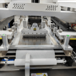
Assembly is usually the tighter constraint. A surface mount line may accept only 400 mm by 500 mm, and anything longer has to be assembled in a special fixture or split into sections that are joined afterwards. Deciding which route to take affects the circuit partitioning long before layout begins.
Fabrication Limits
Drilling a long panel requires registration across the full length, and the accumulated error grows with distance. Equipment that holds 50 µm on a small panel may be specified at 100 µm or more on an oversize one, which reduces the available annular ring on every via.
Plating and etching uniformity are harder to hold as well. Current density and etchant flow vary across a large panel, so copper thickness and line width drift from the centre to the edges. Design rules for long boards should therefore leave margin on minimum line width and on annular ring rather than using the shop’s standard minimum.
Warpage and Stiffness
Warpage scales with the square of the length, so a board of double length is four times as sensitive to an unbalanced stack. Asymmetric copper distribution, uneven dielectric thickness and a single sided design all produce bow and twist that a shorter board would absorb without difficulty.
A balanced stackup is the first defence: copper weights and dielectric thicknesses mirrored about the centre line. Where balance alone is not enough, a stiffener is added. An aluminium or FR-4 backing plate bonded or screwed to the board raises its natural frequency and holds it flat through assembly and service. Mounting features for that backing are part of the outline design described in board outline and mounting design.
Handling During Manufacture
A long, thin panel sags under its own weight, and the sag can crack inner layer copper or disturb registration during lamination. Carriers, edge support rails and careful racking are used through the process, and personnel handling is minimised because a large panel is awkward to move without flexing it.
Automatic optical inspection and electrical test equipment also have size limits. Flying probe testers often handle long boards better than fixtures, because the fixture for an oversize board would be as large as the board itself. Where a bed of nails fixture is unavoidable, the probe plate needs support in the middle as well as at the edges.
Assembly Constraints
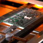
Reflow ovens and conveyors impose their own limits. A board that overhangs the conveyor edges will sag into the oven, and a board that is too wide for the rail system cannot be processed at all. Where an oversize board must be reflowed, it is often supported on a carrier pallet with dedicated support pins under heavy components.
Wave soldering and selective soldering have similar problems, because the board has to sit flat on a pallet with a consistent contact. Component placement also becomes slower: a long board with a small number of parts spread over a wide area spends most of the machine cycle travelling rather than placing.
Signal Integrity on Long Traces
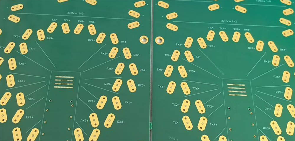
Length brings loss, delay and skew. A signal that travels several hundred millimetres of microstrip loses a noticeable fraction of its amplitude at gigahertz frequencies, and the dielectric contribution to that loss depends on the laminate. Where signals must reach the far end, the material choice and the trace geometry matter more than they would on a small board.
Skew between the members of a differential pair or between a clock and its data becomes significant because the physical distances are large. Length matching has to be planned with the actual propagation velocity of the material, which follows from its dielectric constant. Dimensional behaviour that affects that velocity is discussed in the notes on dimensional stability and expansion.
Ground Planes and Reference Continuity
A long board is usually wide as well, and a wide return path invites plane resonances and noise coupling between distant parts of the circuit. A continuous reference plane with stitching vias along the perimeter, plus local decoupling at each functional block, keeps the impedance low and limits the coupling.
Splitting the board into functional regions with their own decoupling and their own stitching, while keeping a single reference plane underneath, works better than a single global plane with no structure. Where two regions must be isolated, the split should be planned so that no signal crosses it without a stitching capacitor nearby.
Testing and Rework
Access for test is limited by size. Long boards are usually tested with flying probes or with functional test at the edges, and in circuit test is reserved for designs where a full fixture can be justified. Test points should be distributed along the board rather than clustered, so that a fault can be localised to a region.
Rework on a long board is awkward because heating one area distorts another. Preheating the whole board, using localised hot gas and supporting the board on a flat surface all reduce the risk of damage, and the mechanical effects follow the same principles as the laminate behaviour described in the notes on dimensional stability and expansion.
Design Checklist for Oversize Boards
Confirm the maximum panel size the fabricator and the assembly line can handle, then design within it or plan the split. Keep the stackup balanced and specify a stiffener where flatness matters. Leave extra margin on annular ring, line width and spacing, and distribute test access along the length.
Document the mechanical interface: mounting holes, stiffener attachment, bend limits and the flatness requirement after assembly. A long board that is manufactured perfectly but bows in the enclosure will still fail, and the fix belongs in the mechanical drawing rather than in a stronger laminate.
Cost is part of the decision as well. Oversize panels use more material for the same circuit, tooling is more expensive, and the yield loss on a large panel is magnified because one defect can scrap a whole board rather than one of many small ones. Where the product allows, splitting a long circuit into two connected boards is often cheaper than building one oversize panel.
FAQ
What is the practical length limit for a PCB? Most shops can process panels around 600 mm long, and a few handle more than a metre on specialised lines. Assembly equipment is usually the tighter limit at around 400 to 500 mm.
Does a longer board need a thicker laminate? Thickness helps, but a stiffener or a balanced stack usually solves warpage more cheaply. Doubling the thickness increases weight and cost everywhere on the board.
Can a long board be split into sections and joined? Yes, using edge connectors, cables or a continuous flex section, but every joint adds a failure point and an impedance discontinuity. Splitting should be a deliberate design decision, not a workaround found late.