
Copper Plating and Nickel Plating in PCB Fabrication
Two metals do most of the work in PCB plating. Copper forms the conductors and lines every hole, while nickel appears as a thin barrier layer under gold on pads and edge contacts. They are deposited for different reasons, by different processes, and they are judged against different criteria. Confusing the two leads to specifications that ask for the wrong property on the wrong layer.
Why Plating Is Needed at All
Drilling exposes bare laminate inside a hole, so the barrel has to be made conductive before it can be electroplated. That is the job of the electroless copper step, which deposits a thin, continuous layer over the dielectric and the copper foil. Electroplating then builds the layer up to the required thickness on the surface and in the barrel at the same time.
Without plating there is no connection between layers. Every via, every plated through hole and every surface conductor depends on the deposit being continuous, adherent and ductile enough to survive thermal cycling.
Copper Plating Fundamentals
Copper is deposited from an acid copper sulphate bath containing sulphuric acid, copper ions and organic additives. The additives control the deposit at a microscopic level: suppressors slow deposition on the surface, levellers improve thickness uniformity across the panel and brighteners refine the grain structure.
Current density, bath temperature and agitation all influence the result. Higher current density speeds the deposit but can produce a rough, brittle layer; lower current density gives a smoother, more ductile deposit at the cost of a longer cycle. The chemistry that governs this balance is described in the notes on electroplating additives.

Ductility and Barrel Quality
Copper in a plated through hole has to stretch as the board expands during soldering. A deposit with low elongation cracks at the knee where the barrel meets the surface pad, and the crack shows up as an intermittent open long after the board has passed test.
Specifications therefore require a minimum elongation, often 15 to 20 percent, measured on a foil sample plated under the same conditions. Thickness alone does not guarantee quality: a 25 µm barrel with poor grain structure performs worse than a thinner, more ductile deposit. Cross sectioning a coupon from every lot is the standard way to confirm both thickness and structure.
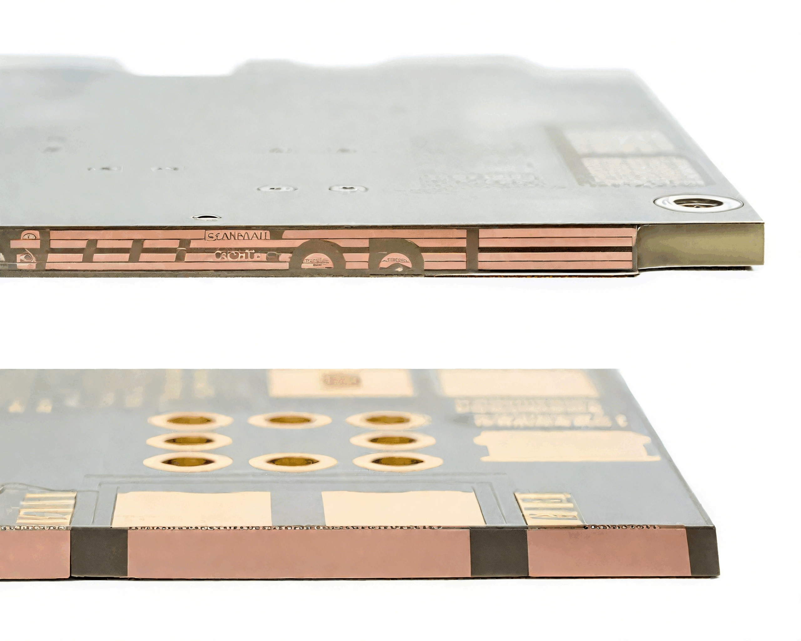
Nickel in PCB Fabrication
Nickel plating is rarely used as a final surface in PCB work, because it passivates quickly and does not solder well. Its value lies underneath. In an electroless nickel immersion gold finish, a 3 to 6 µm nickel layer sits between the copper and a very thin gold layer, acting as a barrier that stops copper from diffusing into the solder joint and providing a hard, corrosion resistant base for the gold.
On edge connectors and hard gold contacts, an electrolytic nickel layer of 2.5 to 6 µm is plated first and hard gold is deposited on top. The nickel carries the wear resistance; the gold provides a stable, low resistance contact surface. Nickel also appears as a barrier in some flexible circuit constructions, where it limits copper migration.
Nickel as a Diffusion Barrier
Copper diffuses readily into solder and into gold at soldering temperatures. Without a barrier, the copper layer under a pad thins over time and brittle intermetallic compounds grow at the interface, weakening the joint. The nickel layer blocks that diffusion because its own intermetallic growth with tin is slow.
The barrier only works if it is continuous. A porous or incomplete nickel deposit lets copper through at the gaps, and the failure appears as a localised weak joint rather than a general one. Thickness matters for the same reason, which is why the nickel layer is specified as a range rather than a single figure.
Deposition Methods Compared
Electroless nickel deposits without current, using a chemical reducing agent, and covers isolated pads evenly because there is no current distribution to worry about. It is the standard choice for a selective finish applied after solder mask. Electrolytic nickel needs an electrical connection to every pad, deposits faster and produces a harder layer, which is why it is used for the whole panel or for an edge contact that will be plugged and plated.
Copper exists in both forms as well: electroless copper for the initial conductive layer and electrolytic copper for the main deposit. A panel therefore passes through several plating tanks, and the sequence matters as much as the chemistry in each one. The defects that arise when a step goes wrong are catalogued in the review of copper plating defects.
Measuring Thickness and Quality
Surface thickness is measured by X-ray fluorescence, which is fast and non destructive, or by coulometric methods on a sample. Barrel thickness can only be seen in a cross section, which is why coupons are plated with every production panel and sectioned for measurement.
Adhesion is checked by tape test or by thermal stress: the coupon is floated on molten solder and then inspected for cracks, blisters and separation. Ductility is measured by tensile testing a plated foil. Together these tests describe the deposit far better than a single thickness number, and they are the reason plating is treated as a controlled process rather than a bath that runs until something looks wrong.
Common Defects
Nodules and roughness come from particles in the bath or from excessive current density. Voids in a barrel come from poor agitation or from air trapped in a deep hole. Skip plating, where an area receives no deposit, usually points to contamination or to a break in the electroless layer.
Stress related defects appear after thermal cycling. Cracks at the barrel knee, pad lifting and barrel separation all indicate a deposit that was too brittle or too thin at a critical point. Where the deposit has to fill a via completely rather than line it, as in via filling for HDI, the control requirements become tighter still.
Specifying the Layers
State the finished copper thickness on the surface and in the barrel separately, the minimum elongation, and the nickel and gold thickness ranges for any finished pads. Name the finish on each side of the board and on any edge contact, and state the maximum number of reflow cycles the finish must survive.
A specification written this way gives the fabricator something measurable to work to, and it gives the assembly house a basis for judging whether a delivered board will survive the soldering process. Vague references to a plating class, without the numbers behind it, leave both sides guessing.
FAQ
Why is nickel used under gold rather than gold directly on copper? Copper diffuses into gold and into solder, which weakens joints over time. Nickel blocks that diffusion and provides a hard surface for a thin gold layer to sit on.
How thick should copper in a hole be? A common requirement is 20 to 25 µm, combined with a minimum elongation of 15 to 20 percent. Thickness and ductility are specified together because either one alone can fail.
Is electroless nickel the same as electrolytic nickel? No. Electroless nickel deposits chemically without current and suits selective finishes; electrolytic nickel requires a current path, deposits faster and is harder, which suits edge contacts and full panel plating.