Running a Pre-Release PCB Design Review
Most board re-spins are not caused by a clever circuit that did not work. They are caused by a footprint with the wrong pad spacing, a connector placed too close to its neighbour, a silkscreen reference sitting on top of a via, or a return path that nobody looked at because the schematic was correct.
A structured design review before the files leave the engineering group catches that class of problem in an hour instead of a week. This article sets out what the review should cover, in the order that a layout actually gets built, and how to run it as a process rather than as a last-minute read-through.
Component Footprints and Pad Geometry
The review starts with the parts, because an error here cannot be fixed by any amount of good routing. Every footprint should be checked against the mechanical drawing for the real part, not against a library symbol that has been copied between projects for years. Pad spacing, pad size, the size of the hole for a through-hole part and the courtyard all need to match.
Through-hole pads deserve particular attention on the drill side. The hole must be large enough to accept the lead with a margin, and a finished hole that is only marginally bigger than the lead will make insertion difficult and the solder joint inconsistent. A generous allowance of roughly 0.2 millimetres over the lead diameter is a reasonable starting point for most pin sizes.
Placement Rules That Prevent Rework
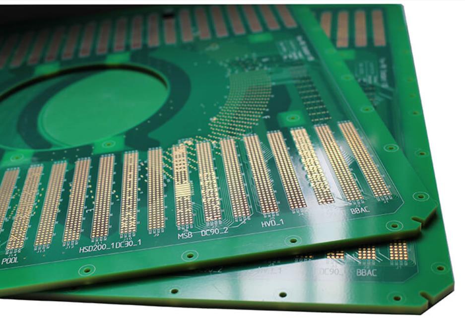
Placement is where a review earns its money. The group of parts that form one function should sit together, and the small parts that belong to a device should sit next to the pin they serve rather than wherever there was space left. A decoupling capacitor that is five millimetres from the pin it decouples is a decorative component, not a functional one.
Connectors need their own check. Their position should follow the mechanical assembly, which usually means the board edge, and their orientation must be correct, because a header that faces the wrong way forces a new cable rather than a new board. The orientation of a connector is not something a netlist can verify, which is exactly why it belongs on the review list.
Keep-Out Zones and Mechanical Interference
A keep-out is a promise to the mechanical design, and components that violate it are usually discovered at final assembly when the fix is expensive. Mounting hardware, screws, standoffs, the inside of the enclosure and the sweep of any moving part all need to be represented on the layout, and the zone must be checked for parts, vias and tall components, not just for copper.
Distance from the board edge matters too. Components placed hard against the routing path can be damaged by the cutter, and a large device such as a controller placed against the edge is more likely to suffer mechanical stress in service. Height is the other dimension that is routinely forgotten: a tall electrolytic capacitor under a low enclosure roof will pass every electrical check and still not fit.
Routing Checks: Width, Differential Pairs and Return Paths
Trace width is an electrical and a process decision at the same time. It must be wide enough to carry the current within an acceptable temperature rise and wide enough for the fabricator to etch, and the two limits can point in opposite directions on a fine-pitch board. A useful sanity check is roughly one millimetre of width per ampere for external traces, adjusted downward for inner layers where the copper is thinner and heat cannot escape.
Differential pairs are checked for equal length, constant spacing and the same layer from end to end. What matters more than any single rule is the return path: every fast signal needs a continuous reference plane beneath it, and a route that jumps across a plane split changes impedance abruptly and radiates. The length matching rules used for serpentine routing are a useful reference here, since they also describe where a length adjustment must not be placed.
EMC and Signal Integrity Review Points
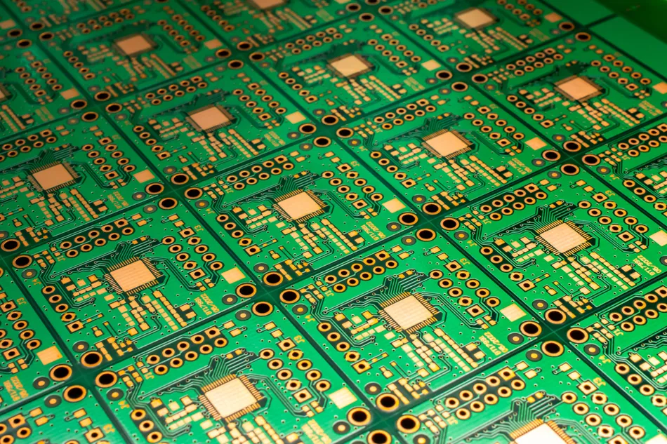
Most of the EMC review is about geometry rather than about filters. The loop area between a fast signal and its return path should be minimised, which means keeping the two close together and avoiding detours around obstacles. Series termination at the driver, or a small capacitor at an input connector, is cheap insurance, but it should be placed deliberately rather than added after the first failed test.
Separating the aggressors from the victims is the second theme. Switching supplies, clocks and high-current switching nodes should sit away from resets, references and analogue front ends, and a ground area between the two groups helps. Analogue traces should be short and should not run parallel to a digital bus for any distance, because coupling is proportional to the length over which the two run side by side.
Silkscreen, Mark Points and Assembly Data
Silkscreen is a manufacturing document, and it should be treated as one. Board name, revision, date and part number belong on the board, along with pin-one marks and any polarity indicators. Reference designators must be readable and must not sit on a pad or a via, because the ink is removed over exposed copper and the marking disappears exactly where it is needed.
If the board is to be machine assembled, at least two or three mark points belong on it, placed so that they are visible after the parts are fitted and not hidden under a tall component. Pin-one and polarity marks on connectors are also part of the assembly data. Reviewing the marking alongside the placement means the operator has the information they need without a separate instruction sheet.
Running the Review as a Process
A checklist is only useful if someone owns it. The practical arrangement is a review meeting with the layout engineer, the hardware designer and whoever will build or test the board, using a projected view of each layer in turn rather than a printed schematic. Going layer by layer catches what a net-by-net review misses, because many of the errors are geometric.
The output should be a list of findings with an owner and a disposition, not a general impression that the board looks fine. Findings that are accepted as risks should be recorded as such, with the reason, so that the same discussion does not repeat on the next revision. Reviewing the characteristics that define PCB quality at the same time turns the meeting into a useful check against the fabricator expectations as well.
FAQ
How long should a design review take? For a moderate board, an hour of focused layer-by-layer review is enough to catch the systematic errors. The value comes from doing it consistently before release rather than from spending a whole day on it once.
Which single check catches the most problems? Footprint verification against the manufacturer drawing. Pad spacing, hole size and courtyard errors survive every electrical check and only appear when the parts are placed, which is the most expensive moment to find them.
Should the fabricator and assembler see the design before release? Yes, whenever the design pushes a limit. A manufacturability review against the actual process capability costs a day and routinely removes a week from the first build.