Metal Core PCB Thermal Design for LED Boards
When an LED board runs hot, no amount of clever routing fixes it. Heat leaves the die through the package, crosses the solder joint and the board, and finally reaches the air. Every one of those steps has a thermal resistance, and the largest one usually sits inside the board itself. That is why metal core PCB designs take shape before the layout does: the copper thickness, the insulation layer, and the area available for spreading heat are decided by the thermal budget, and only then does the routing follow.
Why Thermal Design Comes Before Layout
The starting point is not the heatsink but the junction temperature. Work backwards from the maximum junction temperature of the device, subtract the ambient inside the enclosure, and what remains is the total thermal budget for the path in between. Split that budget across the die attachment, the package, the solder joint, the board, and the heatsink. The board is the step a designer actually controls, so it is where the budget is spent or wasted. If the enclosure sits at 50 degrees and the junction limit is 125, the entire path has to fit inside 75 degrees at full load.
Most LED products are sealed, so natural convection is the only cooling mechanism available. That single fact changes the priorities: radiation and conduction start to matter more than airflow, and surface finish, orientation, and fin spacing become design parameters rather than cosmetic choices. A layout that assumes a fan will fail in the field, because the fan is not there.
<img src="https://www.gopcba.com/wp-content/uploads/2026/09/246.png" alt="Metal core PCB thermal design cross section with aluminum substrate” />
How a Metal Core PCB Is Built
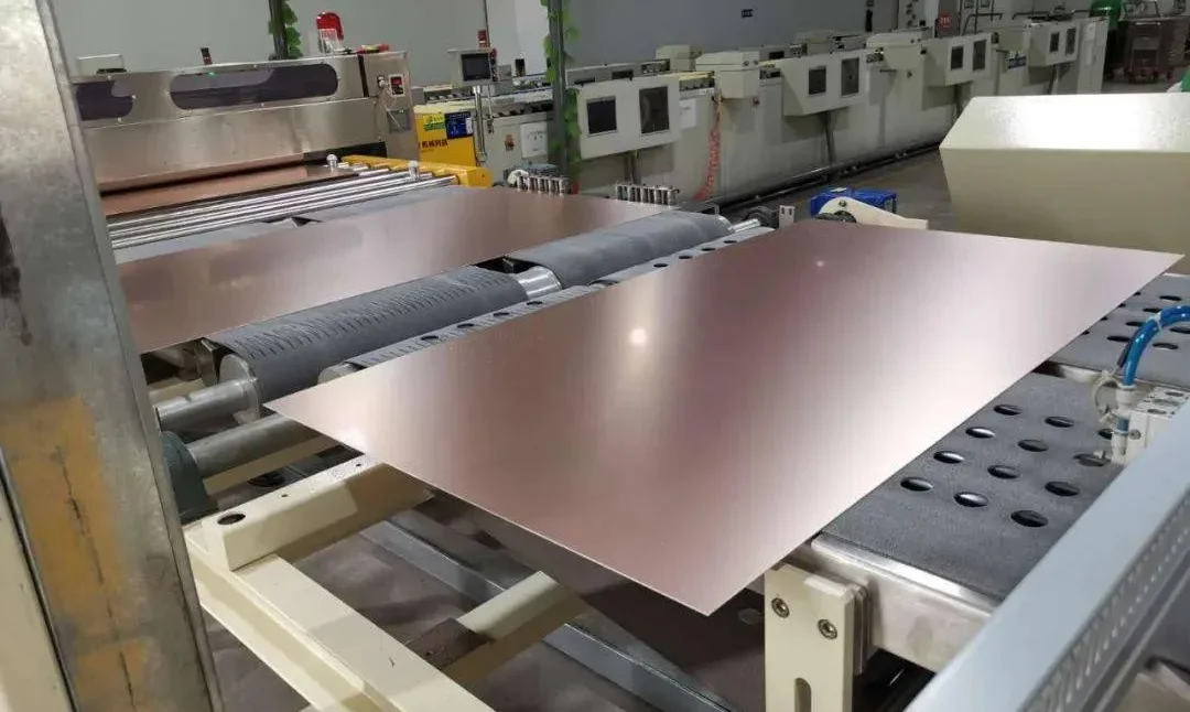
A metal core PCB is a sandwich with three functional layers. The circuit layer is copper foil, normally between 35 and 280 microns, chosen to carry the current without excessive temperature rise. The dielectric layer is the technical core: a ceramic-filled polymer thin enough to keep thermal resistance low while still providing electrical isolation and enough elasticity to survive thermal cycling. The base is a metal plate, usually an aluminum substrate, which supports the assembly and spreads the heat sideways.
The dielectric is where the trade-off lives. Thinner means lower thermal resistance, but the same layer must hold off the working voltage and survive the expansion and contraction of every thermal cycle. A one mil dielectric that withstands more than 2,000 V covers most low-voltage lighting applications, and going thinner buys very little thermally once the copper spreading is adequate. The layer also has to be tough enough not to crack when the board is punched, drilled, or cut, which is why the mechanical properties appear in the same datasheet as the thermal ones.
Choosing Copper and Insulation Thickness
Heavier copper helps twice. It lowers the resistance of the traces, so less heat is generated in the first place, and it spreads heat laterally so that neighboring devices share the burden. When several LEDs sit on the same strip, the copper between them is effectively a thermal bridge. Given the option, prefer a thicker circuit layer and wider traces over a marginally lower thermal resistance in the dielectric.
The practical limits come from the fabrication process. Heavy copper needs wider minimum features, because thick foil etches with more undercut, and the minimum trace and gap both grow. A design that uses the current carrying ability of the trace itself, as described in trace width and current calculation, should confirm the width against the copper weight actually being purchased, not against a default from a different stackup.
Heat Sink Geometry for Natural Convection
Air heated by a surface becomes a boundary layer that clings to it and insulates it. In still air that layer is thick, and it is the reason fin spacing matters more than fin count. Space fins too tightly and the boundary layers of adjacent fins merge, so the air between them stops moving and the extra surface area contributes almost nothing. For a naturally cooled heatsink, spacing above roughly 12 mm keeps the layers separate on a typical extrusion.
The shape of the fin matters less than the surface finish. Adding ripples or serrations to a fin that is cooled by still air changes the flow very little, because there is not enough air movement for the texture to disturb. What does help is a dark, matte finish. A blackened surface radiates more energy at the same temperature, and in a sealed enclosure radiation can carry a meaningful fraction of the total heat. The other useful step is orientation: vertical fins with an unobstructed path above and below them work with buoyancy, while horizontal fins trap their own hot air.

Fin Spacing, Height and Base Thickness
The design sequence for a natural-convection heatsink is short. Define the outline from the mechanical constraints of the enclosure, then optimize the fin thickness, fin shape, fin spacing, and base thickness against the thermal target, and finally verify the result with a calculation or a simulation. Skipping the verification step is common and expensive, because the geometry that looks generous on a drawing is often limited by the base rather than the fins.
Base thickness is the part most often under-designed. Natural convection reaches thermal equilibrium slowly, so a thin base heats and cools faster than the fins can respond. A base and fin thickness above about 5 mm gives the heatsink enough thermal mass to absorb a transient load, such as an inrush period or a dimming event, without letting the junction spike. Below that, a brief overload can push the die past its limit even though the steady-state calculation passed. The same principle, applied to copper rather than to aluminum, appears in copper flooding, mesh or solid, where solid copper is chosen for spreading and mesh for other reasons.
What Heat Does to Components
The reason for all this work is not the LED alone. Elevated temperature degrades insulation and accelerates the aging of every material in the assembly. Resistor values drift, electrolytic capacitors lose life quickly with every additional ten degrees, and the insulation system of a transformer or choke is normally rated below 95 degrees. Heat also changes the solder joint itself: intermetallic growth at the interface thickens over time, and a thick intermetallic layer is brittle and mechanically weaker than the joint that was inspected at the factory.
Semiconductors add a feedback loop on top of that. In a bipolar device, higher junction temperature raises the current gain, which increases collector current, which raises the junction temperature again. The loop settles only because the external circuit limits it, and when the thermal path is too weak it settles at a temperature the package cannot tolerate. This is why the thermal design targets every component in the assembly, not just the one that produces the most heat.
Checking the Design Before Tooling
Before releasing a metal core PCB for fabrication, verify the mechanical interface as carefully as the thermal numbers. The metal base is stiff and flat, but it is also conductive, so the mounting hardware and the enclosure both become part of the electrical environment. Confirm where the board touches the chassis, whether a thermal interface material is required, and how the board is fixed without introducing a bending load. Mounting details that seem unrelated to heat often decide the final temperature, because a board that bows away from its heatsink loses contact exactly where the heat needs to leave; the patterns that avoid this are covered in board outline and mounting design.
The last check is documentation. Record the dielectric thickness, the copper weight, and the thermal resistance that the design assumes, so that a later cost reduction does not quietly substitute a thicker dielectric and erase the margin. Thermal performance is a stack-up property, and it survives only as long as the stack-up does.
FAQ
Do I always need a metal core board for an LED design? No. Low-power LEDs with generous copper on FR-4 often run cool enough. Metal core becomes worthwhile when the thermal resistance of the laminate, rather than the heatsink, is what limits the junction temperature.
Is a thinner dielectric always better thermally? It lowers thermal resistance, but it also has to hold off the working voltage and survive thermal cycling. Below about one mil the thermal gain is small and the isolation margin shrinks.
Why is fin spacing more important than fin count in still air? Because adjacent boundary layers merge when the gap is too small, so the air between the fins stops circulating and the added area stops contributing.
How thick should the heatsink base be? Above roughly 5 mm for a naturally cooled design, so the base has enough mass to absorb transient loads without letting the junction temperature spike.