FPC ENIG Surface Finish: Electroless Nickel Immersion Gold in SMT Soldering
Flexible circuits rarely fail because the copper itself gives up. They fail at the interface, where a thin stack of nickel and gold has to survive reflow, repeated bending and years of thermal cycling. FPC ENIG, the finish most flex suppliers specify by default, exists entirely to make that interface predictable. Knowing what each layer actually does is the difference between a stable assembly and one that dewets on the first production run.
What FPC ENIG Really Consists Of
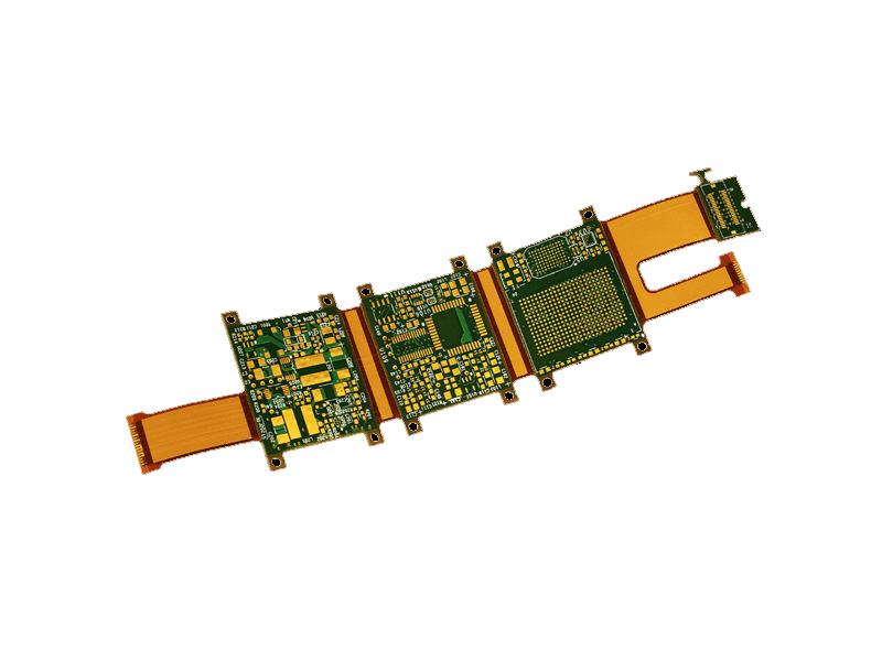
The finish arrives as two metallic layers produced by two different chemistries. The first is a nickel-phosphorus alloy grown by chemical reduction. The second is a very thin gold film formed by a displacement reaction that stops on its own. Because the layers are created by different mechanisms, their thicknesses behave differently during processing, and that difference explains most of the soldering behaviour seen on an assembly line.
Shorthand calls the stack chemical nickel gold, which hides an important fact: the gold is not the soldering surface. Its job is narrower and purely protective. It keeps the nickel from oxidising between fabrication and assembly, and it provides a noble surface for contact or bonding. Every process decision that follows starts from that division of labour.
How the Nickel Layer Forms Without External Current
The nickel deposit is autocatalytic. Sodium hypophosphite in the bath supplies electrons to nickel ions at an activated copper surface, so metal builds up with no rectifier and no bus bar. The result is not pure nickel but an alloy carrying roughly seven to ten percent phosphorus, and that phosphorus content is what gives the deposit its corrosion resistance and its non-magnetic character.
Because the reaction is chemical rather than electrolytic, it covers isolated pads, internal traces and fine-pitch features uniformly. That uniformity is a major reason electroless nickel immersion gold dominates on flex. Electrolytic plating on a thin polyimide substrate requires current to reach every feature, and the resulting thickness distribution across a large panel is far harder to control.
Why Immersion Gold Thickness Is Self-Limiting
Immersion gold is a displacement reaction with a built-in ceiling. Gold ions take electrons from the nickel surface and deposit as metal, while an equivalent amount of nickel dissolves into the bath. Once gold covers the nickel completely, the reaction has nothing left to act on and stops. Practical immersion gold thickness therefore lands between about 0.05 and 0.15 micrometres, and no amount of dwell time changes that.
Thicker gold needs different chemistry, an electroless gold bath with its own reducing agent. That route costs considerably more and is rarely used on flex. Because the immersion layer is so thin, it cannot conceal a defective nickel surface, and it contributes almost nothing to wear resistance. Where abrasion matters, a hard gold deposit over nickel is the correct choice instead.
The Metallurgy of an ENIG Solder Joint
During reflow, molten solder dissolves the gold in a fraction of a second. Intermetallic compounds such as AuSn and AuSn2 form and then disperse into the bulk of the joint. What remains is a connection built on nickel, where tin and nickel react to create a Ni3Sn4 intermetallic layer. The strength of the joint depends on that layer, and the gold has already left the scene.
This is why a Ni3Sn4 intermetallic that is too thick, too porous or interrupted becomes a reliability problem. It grows fastest at high reflow temperatures and with repeated excursions through the oven. A thin, continuous, well-formed layer is the objective, and it comes from clean nickel and a controlled thermal profile rather than from extra gold.
Nickel Thickness and Solder Joint Reliability
Nickel thickness is the single most influential variable on the pad. Below roughly three micrometres the deposit becomes discontinuous along grain boundaries, and the barrier that was supposed to stop copper diffusion develops gaps. Solder joint reliability then depends on a nickel layer that can be consumed during the first reflow, leaving nothing to bond to on a second pass.
Most flex fabricators target three to five micrometres of nickel, measured on the pad rather than on a test coupon. Coupon measurements flatter the process because chemistry and current reach a coupon differently. When a customer asks for a thickness figure, the answer should state where it was measured and by which method, X-ray fluorescence or cross-section.
Black Pad and Other ENIG Failure Modes
The best known defect is black pad. Corrosion of the nickel surface under the gold leaves a phosphorus-rich, poorly solderable layer that appears dark in cross-section. Joints formed over black pad fracture at the interface under thermal cycling, and because the gold still looks normal, the defect is invisible until boards fail in the field.
Other failure modes follow the same theme. A hyperactive or contaminated bath corrodes nickel faster than gold can cover it. Nickel that is too thin exposes copper. Gold porosity lets the underlying nickel oxidise in storage. Solderability testing, cross-sections and scanning electron microscopy remain the practical way to separate a cosmetic concern from a real one.
Choosing a Flex Finish: ENIG, OSP and Hard Gold
The realistic alternatives are OSP, immersion tin, immersion silver and hard gold, plus newer stacks that insert a palladium layer. OSP costs least and suits high-volume consumer flex assembled quickly, but it offers no wire-bonding capability and limited shelf life. Immersion silver solders well and is flat, though it tarnishes and needs sulphur-free packaging.
A practical rule of thumb: use OSP where cost dominates and assembly follows immediately, ENIG where mixed technology, fine pitch or wire bonding is involved, and hard gold on connectors and sliding contacts. Bending flex also deserves attention, since a brittle nickel layer placed in a dynamic bend zone will crack; keeping plated areas near the neutral axis avoids that. Solder alloy choice is covered in lead-free versus leaded solder, pad geometry in PCB pad design standards, and finished-board protection in conformal coating and board protection.
Process Control Points Worth Auditing
Bath maintenance matters more than any specification line. Hypophosphite concentration, pH, temperature and nickel ion level all drift with throughput, and each of them alters the phosphorus content and the corrosion behaviour of the deposit. A supplier who can show bath analysis records is usually a supplier with a stable process and predictable solderability, which matters more on flex than on rigid boards because the substrate cannot tolerate aggressive rework.
Control also extends to what happens before and after plating. Copper that has oxidised or carries resist residue activates unevenly, so the nickel grows at different rates across the panel. A weak rinse after the gold bath leaves salts that attack the finish in storage. For boards that will sit in inventory, packaging and desiccant choice deserve the same attention as the plating line itself.
FAQ
How thick should the nickel be under immersion gold? Three to five micrometres is the working range for most flex and rigid boards. Thinner deposits risk discontinuities and copper diffusion, while much thicker nickel adds brittleness and cost without improving the joint.
Can gold thickness be increased for repeated reflow? Only by switching to an electroless gold bath. Immersion gold is self-limiting, so extending dwell time will not add thickness. If a board sees three or more reflow passes, control nickel quality and the thermal profile instead.
Why does solder sometimes dewet on ENIG pads? The usual cause is a compromised nickel surface rather than the gold. Black pad, an over-active bath, contamination before plating or excessive storage time can all leave a nickel layer that molten solder refuses to wet, even though the pads look perfectly gold.