High-Frequency PCB Materials and Hybrid Stackups
A high-frequency PCB is usually described by its material rather than by its geometry, and that emphasis is correct. Once a signal spends a meaningful part of its energy in the laminate instead of the copper, the loss tangent of the dielectric, not the width of the trace, sets the budget. The rest of the design follows from that: which laminate to use, where a hybrid stackup earns its cost, and how the vias are filled so that the impedance stays continuous from top to bottom.
What Makes a Laminate Suitable for High Frequency
Four properties decide the question. The dielectric constant sets the impedance for a given geometry, so it has to be known to the accuracy the design needs, not to the nearest tenth. The dissipation factor sets how much energy is turned into heat per unit length, which is why it matters more than the dielectric constant on long runs. Stability matters next: both values have to stay reasonably constant over frequency, humidity, and temperature, because a laminate that drifts forces the design to hold margin it may not have. Finally, the glass transition temperature and the processing behavior determine whether the material can survive the fabrication sequence at all.
These four properties explain where high-frequency laminates are used. Antennas, base station receivers, power amplifiers, splitters, combiners, and filters all live in a world where a small change in dielectric constant shifts a resonant frequency, and radar and navigation hardware adds a thermal requirement on top. In each case the design intent is a low-loss, well-controlled transmission path, and the material is the first decision that supports it.

Classifying Copper-Clad Laminate
Copper-clad laminate is described by three components: the copper foil, the reinforcement, and the resin system. Reinforcement separates the two large families. Glass cloth and glass mat sit on one side, paper on the other, which is why laminates are loosely grouped into glass-based and paper-based types. The resin determines the rest of the behavior: phenolic, epoxy, polyester, polyimide, and PTFE each produce a different balance of cost, temperature range, and electrical loss.
The same laminate is then classified by how it behaves, not just what it contains. Type by flammability, rigid or flexible by construction, and heat-resistant, radiation-resistant, or high-frequency by application. Metal-based laminates appear in the same catalog, as do foils other than copper where a specific resistance or thermal expansion is needed. Reading a datasheet properly means knowing which of these axes the design is sensitive to.
When a Hybrid Stackup Makes Sense
A board rarely needs low loss everywhere. Digital control, power conversion, and housekeeping circuits are perfectly comfortable on ordinary FR-4, while two or three signal layers carry the microwave path. A hybrid stackup places high-frequency material only where the lossy lines run, and laminates the rest from the cheaper material, which controls cost without compromising the electrical performance that mattered.
The trade-off is in fabrication. Mixing two materials means matching their coefficients of thermal expansion, their thickness tolerances, and their processing temperatures, and it usually means asymmetric builds that are harder to keep flat. Choose it when the alternative is a full high-frequency stack where only a fraction of the layers benefit, and keep the number of distinct materials to a minimum. General guidance on how layers should be ordered is in layer stackup from one to eight layers.
Resin Plugging for Buried and Blind Vias
Buried and blind vias that sit under a component land have to be filled before the next layer is laminated, and the sequence is specific. The via is drilled and plated, then filled with a resin, then baked, then ground flat. Because the ground resin contains no copper, a further plating step is needed to bring the surface back up to a pad. All of this happens before the remaining holes are drilled, so the plugged vias are finished first and the rest of the board then follows the normal process.
The filling has to be complete. A void left inside the plug traps moisture, and trapped moisture is the mechanism behind the delamination and blistering that appear when a board passes through a reflow or wave soldering oven. Baking drives some of it out, but the same baking step also pushes resin out of the hole when the void is large, leaving a surface that is concave on one side and proud on the other. That is at least inspectable. The dangerous case is the small void that survives, and the practical defense is to bake the panels before soldering rather than to rely on the fill alone. The process and its variants are described further in electroplating and via filling in HDI.
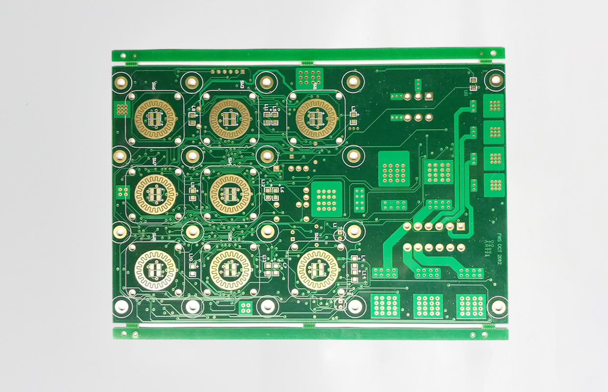
Voids in Filled Vias
A cheaper alternative to resin is to plug the vias with solder mask ink during the normal mask operation, either before or after the surface ink is printed. It fits the existing flow and costs almost nothing, but the quality is lower: the ink shrinks during curing, so a hole that looks full when it leaves the printer is slightly recessed after the bake. For a design with a demanding requirement for fill flatness, ink plugging will not meet it, and resin is the only option that does.
Whichever material is used, the requirement should be stated on the drawing. Whether a via must be filled and capped, filled and planarized, or simply tented changes the number of process steps and the price, and a fabricator who has to guess will choose the cheapest interpretation that satisfies the artwork.
Design Checklist for a High-Frequency Build
Before release, confirm four things. Check that the dielectric constant used in the impedance calculation matches the material being purchased, including its tolerance. Confirm that the hybrid regions are large enough to laminate reliably and that the stack is as balanced as the routing allows. Confirm that every via in a high-frequency path is either filled or excluded from the path, since an unfilled via is an impedance discontinuity. Finally, confirm that the surface finish and the soldermask process are compatible with the laminate, because PTFE-based materials need specific preparation to bond. The broader set of via choices is compared in via in pad or plated through.
One more material decision belongs on that checklist: the copper foil itself. Standard electrodeposited foil is adequate for most high-frequency work, but its surface roughness contributes to loss at the highest frequencies, because current crowds into the peaks of the foil profile. A smoother or reverse-treated foil presents a low-profile surface to the dielectric and reduces that contribution. The effect is small at a few gigahertz and grows quickly above ten, so it is worth checking whether the loss budget actually depends on it before paying for the upgrade. If the design is already close to its limit, the foil is one of the cheapest remaining levers.
FAQ
Why is dissipation factor more important than dielectric constant on long lines? Because the dielectric constant sets the impedance, which can be tuned by geometry, while the dissipation factor sets the loss per unit length, which cannot be recovered once the material is chosen.
When is a hybrid stackup worth the extra process steps? When only a few layers carry the high-frequency path. If most of the stack benefits, a single high-frequency material is simpler and often cheaper overall.
What causes blistering on a board with filled vias? Moisture trapped in a void inside the fill. It turns to steam in the soldering oven, and the pressure separates the layers.
Can solder mask ink replace resin for via plugging? Only where flatness does not matter. The ink shrinks during cure, so the fill ends up slightly recessed.