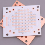
Custom Shape PCB: Outline Design and Milling Tolerance
Not every board is a rectangle, and once the outline stops being a rectangle it becomes a manufactured feature with tolerances rather than a boundary. A custom shape PCB is used when the enclosure, the mounting arrangement or the optical path dictates the geometry, and the design work moves from the schematic to the mechanical drawing.
When a Custom Shape Is Needed
Typical cases include a board that follows the curve of a housing, a control panel where the electronics are arranged around a display or a knob, and a wearable or handheld product where the outline is dictated by how it is held. Internal cutouts appear where a battery, a lens or a mechanical shaft passes through the board.
The alternative to a custom shape is usually a rectangular board plus a bracket or a spacer, and the comparison is worth making. A rectangular board with a simple mounting arrangement is cheaper to make and easier to assemble, so the custom shape should earn its cost through a real mechanical or optical requirement.
Outline Tolerances
Milling tolerance is the variation in where the edge of the board actually lands, and outline tolerance is the way that variation is expressed on the drawing. It is set by the routing process, by the registration of the outer layer artwork to the outline and by the stability of the laminate through the process.
A typical figure for a routed outline is around plus or minus a tenth of a millimetre, with tighter values available at higher cost. What matters for the design is not the figure itself but its place in the tolerance stack: if the board locates a connector that mates with a housing, the outline tolerance, the connector placement tolerance and the housing tolerance all combine. The principles are those described in board outline and mounting design.
<img src="https://www.gopcba.com/wp-content/uploads/2026/05/smart-healthcare-PCBA.jpg" alt="Custom shape PCB with curved outline and internal cutout” />
Corner Radius and Internal Cutouts
A router bit has a diameter, so every internal corner is rounded with a radius of at least half that diameter. Specifying a sharp internal corner in the drawing does not produce one, and the fabricator will either use the smallest available tool or ask for a change.
Internal cutouts are routed with a separate tool path, and they need clearance from any copper, from any component and from the board edge. A cutout that passes through a plane or a trace cuts it, so the design has to route around the opening, and the region near the cutout should be checked for mechanical weakness. Where a cutout is close to a mounting hole, the material between them can crack under load.
Copper to Edge Clearance
Copper near the board edge is exposed when the board is routed, which risks a short against a metal housing and creates a corrosion path in a humid environment. The clearance required depends on the voltage and on the application, and for high voltage boards it is a safety distance rather than a manufacturing preference.
The clearance also has a manufacturing dimension. The milling tolerance means the actual edge can be inside the nominal outline, so the copper should be kept further back than the minimum specified by the process. A plane that runs to the outline will be exposed on some boards in every panel.
Fiducials and Handling
An irregular outline can make it harder for the placement machine and the inspection system to locate the board. Fiducials placed outside the board area, in the panel frame, solve the problem for the assembly process, and local fiducials near fine pitch components help the placement accuracy.
Handling features are a practical necessity for unusual shapes. A panel with a curved outline may be difficult to support and to convey, and adding break away rails or tabs keeps the panel stiff until the last operation. The panel design should be agreed with the fabricator and with the assembly house together, since a panel that suits one may not suit the other.
Panel Utilisation and Cost
The outline determines how many boards fit on a panel, and that number drives the unit cost more than almost anything else about the shape. A curved outline leaves material that cannot be used, and closely nested parts risk damage during routing.
Where the product allows it, small changes to the outline can improve nesting considerably. Aligning cutouts between adjacent boards, adjusting a radius or accepting a slightly smaller tab can move a design from an awkward fit to an efficient one, and the saving applies to every unit produced. The broader set of manufacturability choices is covered in PCB design guidelines for manufacturability.
Design for the Enclosure
An irregular board usually has a mechanical function, so the design has to account for how it will be held. Mounting holes, slots, edge contacts and locating features all interact with the outline tolerance, and the design should designate one feature as the datum against which the others are dimensioned.
Where the board slides into a groove in a housing, clearance has to be provided for the outline tolerance at both ends. Where it is clamped, the clamping force must not be taken by a narrow section of board that could crack. Both are mechanical decisions with an electrical consequence if the board is stressed.
Prototyping and Verification
An unusual shape should be verified physically before volume production. A prototype cut on a milling machine or routed from a small panel confirms the fit with the enclosure and the clearance around the mounting features, and it costs far less than tooling.
The check should include the components, not only the bare board. A connector or a tall capacitor near the edge of a curved outline can protrude beyond the intended envelope, and that is only visible when the assembly is built. Where the shape is critical, the prototype stage should use the production components and the production enclosure, and the earlier comments on multilayer PCB prototype requirements apply with more force for a shaped board.
Manufacturing Practice
Routed outlines are produced with a programme that follows the artwork, and the tool diameter is chosen from the smallest internal radius in the design. Where a shape has both fine detail and long straight edges, more than one tool may be used, and the sequence affects the accuracy at the transition.
The fabricator should confirm the achievable tolerance for the specific shape rather than for a generic outline, since a long curve behaves differently from a small cutout. Supplying the outline as a proper mechanical layer rather than as a drawing note removes one class of error at the start.
FAQ
Can any shape be routed? Almost any shape that can be described by a tool path. Limits come from the minimum internal radius, the amount of material that must remain and the handling of the panel.
How tight can the outline tolerance be? Around a tenth of a millimetre is routine, and tighter values down to a few hundredths are available from shops that specialise in it, at a cost that rises quickly.
Is a shaped board more expensive? Usually, because of the panel utilisation and the extra routing time. The premium is often justified by removing a bracket or a spacer from the assembly, which should be part of the comparison.