Any Layer HDI PCB: Stackups, Microvias and Build Sequence
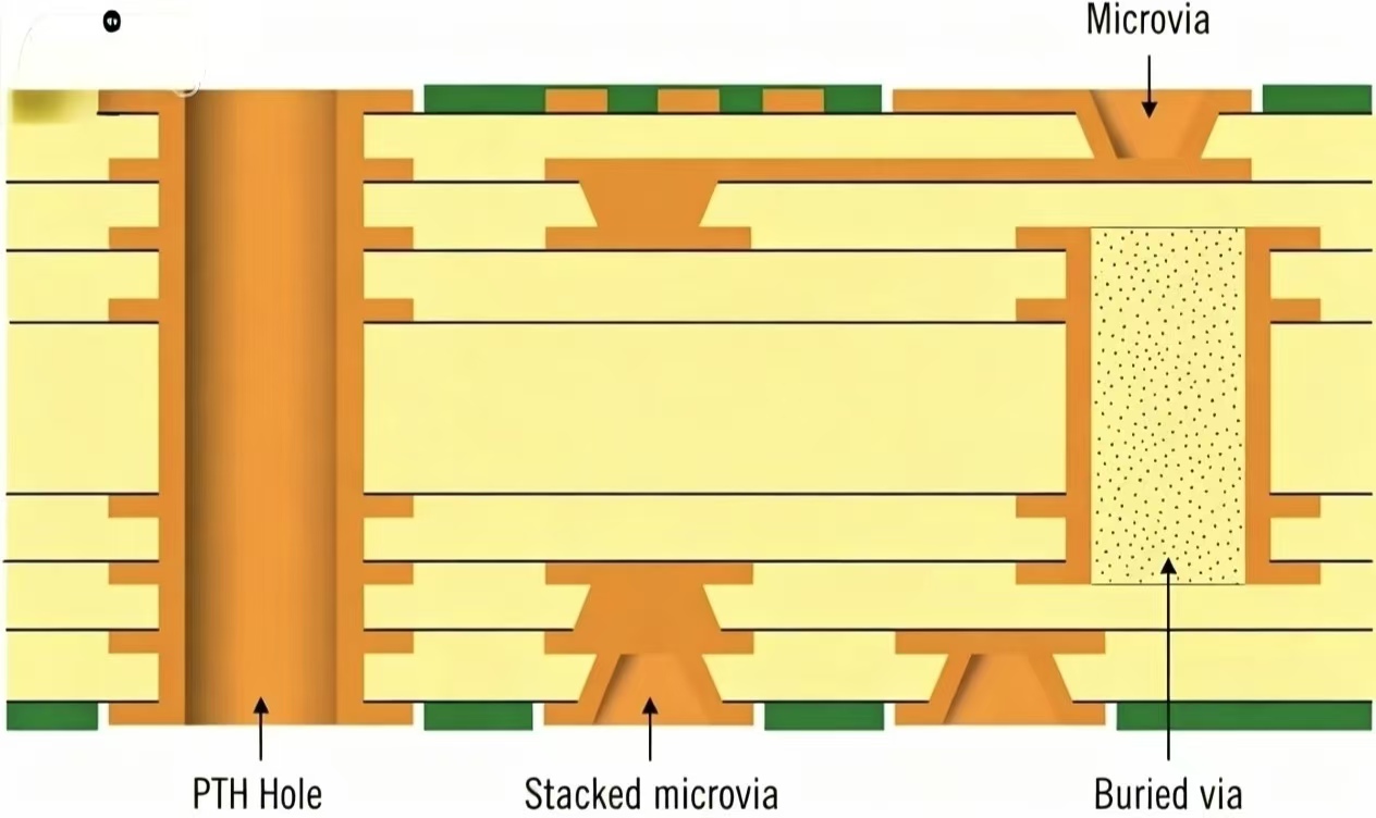
Any layer HDI removes a constraint that older high density designs accepted as a rule. In a conventional HDI stack the microvias connect only the outer layers to the next one, so a signal that has to reach an inner layer is forced through a combination of buried vias and through holes. In an any layer stack, a microvia can be formed between any two adjacent layers, which allows the connection to be made wherever it is needed.
The freedom is real but it is not free. Each microvia adds a lamination cycle, and a stack with several of them has to be built in a sequence that the fabricator can actually execute. Understanding that sequence is what allows a design to use the technology efficiently rather than expensively.
What Any Layer Interconnection Means
The term describes a stack in which every layer pair can be connected by a microvia, not only the pairs next to the two outer surfaces. The vias are formed by laser drilling into a thin dielectric and then plating, and the layers are built up one or two at a time.
The consequence is routing freedom. A signal can travel from a component pad on the top layer to an inner layer without passing through the whole board, which frees the space that a through via would have consumed on every other layer and improves the electrical performance by removing the stub.
Why the Density Is Needed
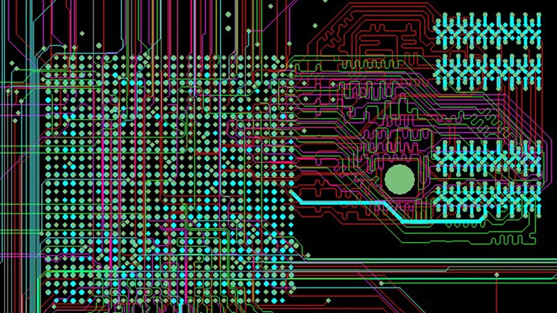
A large ball grid array with a fine pitch presents more connections in one area than a conventional stack can escape. The layers available for routing between the balls are limited, and without microvias the escape routing cannot reach the inner layers within the available space.
The same pressure comes from the component side: a package with a fine pitch needs a pad geometry that leaves very little room for a via, so the via has to be small and, often, placed in the pad itself. That is only possible with a laser drilled, filled and plated over via.
Build Sequences
An any layer stack is built up from a core. The first microvia layer is laminated, drilled and plated, then the next one is added, and the process repeats until the outer layers are complete. Each repetition is a lamination cycle with its own registration, its own dielectric and its own inspection step.
The number of cycles is the main cost driver. A stack with three sequential lamination cycles is significantly more expensive than one with two, and a design that needs a microvia between layers that are not adjacent forces an additional cycle. Aligning the routing with the build sequence is therefore a cost decision as much as a technical one.
Microvia Formation and Quality
Microvias are formed by laser, usually with a copper foil that acts as a stop or with a controlled energy that stops at the target pad. The resulting hole has a conical profile, and its depth to diameter ratio is limited: a typical specification allows a ratio of about 0.75 to 1, which caps the dielectric thickness that can be drilled reliably.
The quality of the via depends on the target pad, the dielectric and the desmear. A via that does not land fully on the pad produces a weak connection, and a via with inadequate desmear has a high resistance that changes with temperature. Both are verified by cross section and by a resistance measurement on a daisy chained coupon.

Design Rules and Routing Strategy
The escape routing is planned from the ball field outwards, with the via positions chosen so that the traces can reach the inner layers without competing for the same channels. Via in pad is used where the pad geometry allows, and the microvia stack is arranged so that consecutive vias are offset rather than stacked, unless a stacked structure is explicitly supported by the process.
Stacked microvias, where one via sits directly on another, are possible but they require a filled and planarised via below, and they concentrate the mechanical stress in the same column. Where the design can tolerate the extra layers, an offset arrangement is more robust and usually cheaper.
Materials and Reliability
The dielectric around a microvia is thin, so the material properties that matter are the ones that govern adhesion and expansion at small scale. A resin with a low expansion and a high glass transition temperature reduces the stress in the via, and a material with good desmear behaviour produces a cleaner barrel.
Reliability is assessed with thermal cycling and with a drop or bend test where the product demands it. The failure mode is a crack at the interface between the microvia and the pad beneath, which is why the target pad size and the surface preparation are specified rather than left to the process.
Cost, Yield and Where It Pays
Any layer HDI costs more per layer than a conventional build, and the cost rises with each sequential lamination. It pays where the density requirement cannot be met another way: a large fine pitch ball grid array, a module with several high density devices in a small area, or a product where the size reduction justifies the board cost.
Where the constraint is less severe, a conventional HDI stack with microvias only on the outer layers often meets the requirement at a lower cost. The evaluation should start from the escape routing, because that is the point at which the two options diverge.
Manufacturing and Inspection
The process control points are the registration between layers, the laser drill energy, the desmear, the via fill and the planarisation before the next lamination. Each of them is verified on a coupon and, for the critical cases, on a cross section of the production panel.
gopcb builds HDI stacks including any layer constructions, with laser drilled microvias, filled and plated over vias and the coupon data that a high density design needs to qualify the process.
Comparing Build Up Options
There is more than one way to build up a high density stack, and the choice between them is made on the required density, the acceptable number of lamination cycles and the available material set. A build up that adds one microvia layer to each side of a conventional core is the least expensive, while a fully any layer structure with several sequential cycles delivers the greatest freedom and the highest cost. Between the two there are intermediate stacks in which the outer two layers on each side are connected by microvias while the centre of the board remains conventional.
Each of those options has a different effect on the escape routing. A structure with two microvia layers on each side can often escape a fine pitch ball grid array without any through via in the ball field, which removes the stub and frees the inner layers for power and ground. Where the field is denser still, the additional freedom of an any layer build up is what makes the routing possible at all, and that is the case in which the extra cycles are justified rather than merely tolerated.
FAQ
What is the difference between HDI and any layer HDI? A conventional HDI stack uses microvias on the outer layers only. An any layer stack allows a microvia between any two adjacent layers, which needs more lamination cycles and gives more routing freedom.
How deep can a microvia be? The practical limit is a depth to diameter ratio of about 0.75 to 1, which is why the dielectric around a microvia is thin and why the layer being connected to is usually the adjacent one.
Are stacked microvias reliable? They are used in production, but they concentrate stress in one column. Where the design allows, an offset arrangement is more tolerant and easier to build.
Related reading: high density interconnect PCB, PCB via plugging, back drilling design, and PCB capture pad design.