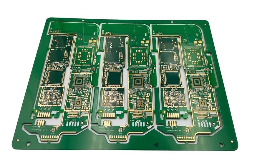
Back Drilling PCB Design: Stub Control for High-Speed Vias
A via that runs from the top of a board to the bottom carries signal only for the part of its length that the signal actually needs. The remainder is a copper stub hanging off the trace, and at 25 Gb/s and above that stub is electrically a resonant element that reflects energy back to the transmitter and eats into the link budget.
Back drilling removes the unused portion of the barrel after plating, and the design decisions that make it work are made long before the drill program is written. This article covers why stubs matter, how the process is controlled, what tolerances to specify and how to choose between back drilling and blind or buried vias.
Why Via Stubs Matter at High Data Rates
A stub behaves as a shorted transmission line. Its impedance and electrical length set a resonance frequency, and near that frequency the return loss of the channel collapses and the insertion loss rises sharply. At 10 Gb/s the effect is visible but manageable; at 56G PAM4 and beyond it can close the eye entirely.
The resonance moves lower as the stub gets longer or the dielectric constant rises. A 60 mil stub in a thick backplane and a 25 mil stub in a thin line card are not equivalent problems, which is why the stub target in a specification is always given together with the layer and the data rate it applies to.
How Back Drilling Works
After plating and before outer layer imaging in many flows, a controlled depth drill enters the board from the side the signal does not use and removes the barrel down to a defined distance from the last layer the signal connects to. The remaining copper is the stub, and its length is the parameter the fabricator tries to hold.
Depth control is the whole discipline. Mechanical back drilling uses a drill with a reduced diameter and a depth stop referenced to the surface or to a detected layer, while laser and depth sensing variants are used where the tolerance has to be tighter. Panel thickness variation across a production lot is the largest single contributor to the error.
Stub Targets and Tolerances
A common engineering target is a residual stub of 8 mil or less for 25 Gb/s class channels and 5 mil or less for 56 Gb/s and above, measured as the electrical length from the last connected layer to the bottom of the drilled hole. The tolerance on that number is as important as the number itself, because a channel is designed against the worst case.
The tolerance also drives cost. Holding 5 mil across a panel requires tight thickness control, a dedicated drill program per stackup and electrical test coupons that verify the result. Relaxing the target from 5 mil to 8 mil can remove a processing step, so the specification should state the maximum that the link can tolerate rather than the tightest number available.
Back Drilling Versus Blind and Buried Vias
Blind and buried vias avoid the stub by construction, since the barrel is only formed between the layers that need it. That is electrically the cleanest solution, but it requires sequential lamination and multiple bonding cycles, which raises both cost and lead time, especially as the layer count grows.
Back drilling is a secondary operation on a conventional through hole stack, so the base construction remains standard and the additional cost is limited to the drilling and inspection steps. For designs between eight and thirty two layers with through vias already in the stackup, back drilling is usually the better trade.

Design Rules That Make Back Drilling Work
The via must be reachable from the side being drilled, so the opposite side has to be clear of components and solder mask openings that a depth controlled drill could damage. Keep a clear annulus around every back drilled via and mark the affected vias in the fabrication drawing rather than relying on the drill file alone.
Vias that share a drill size and a depth requirement are grouped, because each unique combination adds a drill program and a setup. Where a via carries a signal on the very bottom layer, back drilling is impossible and the design has to move to a blind via or reroute the layer assignment instead.
Inspection, Cost and Yield
Because the stub is inside the board, inspection is indirect. Fabricators verify depth with cross sectioned coupons from the same panel, and increasingly with electrical measurements on a test coupon that mimics the channel. Sampling frequency is part of the agreement, and it should be written into the specification.
gopcb supports back drilled stackups with defined stub targets, coupon based depth verification and the impedance control that high speed channels require. The stub target, the layer where the signal terminates and the side to be drilled all belong in the fabrication drawing, and stating them clearly is the difference between a first pass success and a re-spin.
Material and Stackup Considerations
Back drilling changes the economics of the stackup. Reducing the board thickness lowers the residual stub for the same layer count and can remove the need for a tighter depth tolerance, so thickness is worth revisiting before the drill program is fixed. Higher performance laminates help as well, because a lower dielectric constant raises the resonance frequency of a given stub.
Layer assignment deserves the same attention. Signals that need back drilling should terminate on the innermost layers the channel reaches, so the stub that remains is as short as the stack allows, and the fabricator should see the layer map, the via types and the drill side together rather than as three separate notes on a drawing.
Design Review Checklist
Before release, confirm the stub target against the link budget, mark every via that requires back drilling, and state the drill depth tolerance and the layer on which each of those vias terminates. Then check the drill side for components, mask openings and test points, because anything a depth controlled drill could touch is a risk.
Finally, confirm how the result will be verified. Cross sectioned coupons, electrical test structures or a defined sampling plan all work, but the method has to be agreed before the panels are released, since a measurement agreed afterwards rarely matches the number the designer had in mind.
Related reading: high frequency trace routing, via in pad versus plated through, PCB manufacturing tolerances, and microstrip and stripline routing.
FAQ
When is back drilling worth the extra cost? When the data rate is high enough that the stub resonance falls inside the channel bandwidth, typically from 25 Gb/s upward, or when the stackup is thick enough that through vias leave long stubs even at moderate rates.
What stub length should be specified? Eight mil or less is a reasonable default for 25 Gb/s class channels, and five mil or less for 56 Gb/s and above. The number should come from the link budget rather than from habit.
Can back drilling damage the board? It can if the depth control fails and the drill removes copper from a layer the signal still needs. That is why the operation is verified with coupons and why a clear annulus and a clear drill side are specified in the fabrication drawing.