Stepped PCB Manufacturing: Cavity, Controlled Depth and Lamination
A stepped board, also called a cavity board, is a multilayer construction in which part of the outer surface is machined away so that an inner layer becomes the top surface in a defined area. The purpose is mechanical: a tall component such as a bare die, an optical device or a shielding can sits inside the recess instead of on top of the board, which reduces overall height and shortens interconnect length.
Why a Cavity Is Used Instead of a Flat Stack
Height restrictions drive most cavity designs. When a package must sit below the surface of the surrounding circuitry, no amount of stackup planning will achieve it on a flat board, so material has to be removed. Shortening a connection is the second reason: placing a device in a recess lets it sit closer to the inner layer it connects to, which improves electrical performance for high frequency devices.
Mechanically, a cavity also allows a component to be surrounded by board material rather than sitting proud of it. That protects the device, provides a natural shielding boundary and allows the assembly to remain flat for subsequent processing. The trade is a more complex manufacturing sequence, since the cavity must be created without damaging the layers beneath it.
The Stacked Substrate Approach
A practical method builds the board from separately prepared substrates: an upper board, one or more middle boards and a lower board. Each is cut to size first. The inner layer pattern is then formed by image transfer on the lower face of the upper board, the upper face of the lower board and both faces of each middle board, with unwanted copper removed to leave the required circuit pattern.
The middle board is then routed to create a window at the required position and size. This window is what will become the cavity, and its dimensions matter because the recess in the finished board is defined by it. Controlling that opening accurately at this stage is easier than trying to machine the cavity after lamination.
Alignment Holes and Resin Plugging
The substrates are then drilled together to produce a common set of alignment pin holes. Because the layers must register precisely, these holes are the reference that holds the stack together through the remaining operations, and any error in them propagates directly into layer-to-layer alignment.
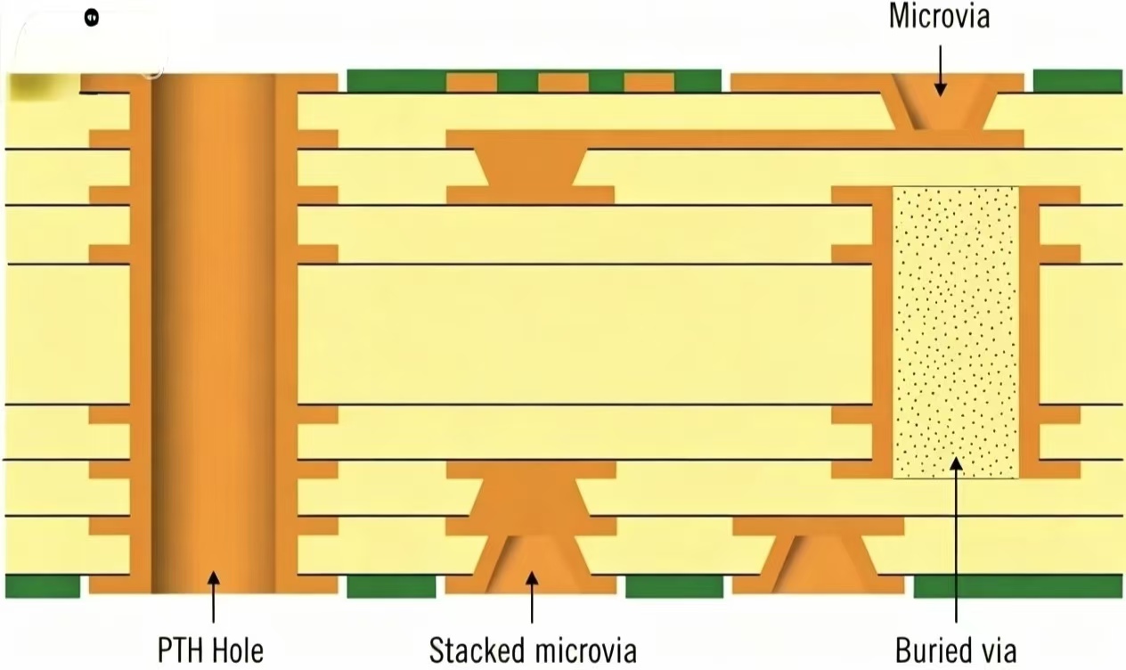
Those same pin holes are selectively filled with resin by printing before lamination. The purpose is to stop resin and plating chemistry from migrating through the stack later, and to keep the alignment holes from becoming unintended electrical paths. Selective plugging, rather than coating the whole panel, keeps the process compatible with the inner layer pattern already formed. The technique and its alternatives are described in resin plugging versus via tenting.
Lamination and the Controlled Depth Step
Prepreg is placed between the layers, the stack is aligned on the pins and the assembly is vacuum pressed at elevated temperature and pressure so that the resin cures and bonds the substrates into one board. Vacuum is used because trapped air between large panels produces voids that later appear as delamination or as blistering during soldering.
Only after bonding is the step itself created. A forming machine cuts the upper substrate to a controlled depth at the cavity location, removing board material until the circuit pattern on the lower substrate is exposed. Depth control is the critical variable: cutting too shallow leaves material that defeats the purpose, and cutting too deep destroys the conductor beneath. Tool wear, depth measurement and a verification cut on a coupon all matter here.
Secondary Drilling, Plating and Outer Layers
With the cavity in place, the board is drilled again using slot cutters of different sizes to produce the required openings. Plating then deposits copper on the outer surfaces and inside those slots, so that the walls of the openings conduct between layers. The cavity walls must plate evenly, which is difficult where the recess shields the solution flow from reaching the surface.
<img src="https://www.gopcba.com/wp-content/uploads/2026/08/assembly-parts-e1599389540536.jpg" alt="Controlled depth routing tool cutting a step into a multilayer board” />
The outer layers are formed in the usual way: dry film lamination, image transfer, alkaline etching, then solder mask printing, legend printing and finally profiling, where the panel borders are removed and the board is cleaned and finished to shape. Each of those steps has to tolerate the cavity, which means that conveyor tooling, vacuum tables and roller pressures must all be adjusted for a board that is no longer flat.
Where Stepped Boards Are Used and How to Specify Them
Typical applications include optical modules, radio frequency front ends, sensor packages and products where an embedded component must sit flush. The common requirement in each case is a defined recess with a controlled floor and a reliable connection to the layer it exposes.
When specifying a cavity, state the finished depth, the tolerance on that depth, the position and size of the opening, and whether the exposed surface needs a specific finish or must remain solderable. Add the mechanical constraints imposed by the surrounding assembly, such as keep-out areas and stack height. Because the sequence is longer than a conventional build, cavity designs benefit from early review; general multilayer process limits are described in multilayer PCB manufacturing challenges and the lamination workflow in the PCB lamination process guide.
Design Rules and Yield Considerations
Cavity geometry is constrained by the material around it. The board must retain enough thickness beneath the recess floor to keep the exposed pattern mechanically supported, and enough material at the sides for the stack to hold together during pressing. A cavity that leaves only a thin web under the floor will survive fabrication but may not survive assembly, particularly if a connector or a mounting screw applies load in that area.
Component placement interacts with the step. Solder paste printing behaves differently across a discontinuity in the surface, so stencils are usually gapped or stepped around the cavity, and placement nozzles need clearance for both the recess and the raised border. Cleaning and inspection also become harder, because fluid can collect in the recess and a camera may not focus on the cavity floor and the surrounding surface at the same time.
Finally, consider the cost of failure. A cavity is created late in the sequence, so a board scrapped at that point has already consumed the value of every inner layer. Yield therefore benefits from conservative geometry, a cavity placed away from the densest routing, and a first article that is sectioned to confirm both the depth and the bond quality around the opening.
FAQ
How deep can a cavity be cut? The limit is set by the thickness of the material above the layer to be exposed and by the tolerance the process can hold. Cutting to expose an inner layer pattern is common; cutting into or through a conductor is not acceptable, so depth tolerance is the controlling specification.
Why are the alignment holes resin plugged? To prevent resin and chemistry from travelling through the stack during lamination and plating, and to stop the holes becoming accidental conductive paths between layers.
Does a cavity change how the board is assembled? Yes. The recess affects paste printing, placement and reflow, and it interacts with the panel design, so the cavity should be documented in the fabrication drawing and reviewed with the assembly house.