PCB Layout Order: Four Position Classes to Fix Before Routing
Most first-pass layout sessions stall for the same reason: the schematic is finished, the netlist is imported, and a screen full of rat’s nest lines gives no hint about which part should move first. Some engineers drop the largest chip into the middle of the board, others line the connectors along one edge, and the rest fill whatever gap is closest. A repeatable PCB layout order removes that guesswork. Instead of tidying parts, you sort positions into four classes: the ones that cannot move, the ones that must sit near their partners, the ones that serve a specific device, and the space that future routing and assembly will need.
That order is not a style preference. It follows from what a board actually is at the same time: a mechanical part, an electrical network, and a manufactured assembly. Fixing the mechanical constraints first prevents late rework, grouping functional blocks keeps the connection paths short, and reserving access space avoids a redesign after routing fails. On a small low-voltage practice board the sequence takes a few minutes; on a product with an enclosure it decides whether the project stays on schedule.
Class One: Positions You Cannot Move
Start from the outline and the mechanical requirements, not from the device sizes. Mounting holes, a button that must line up with a cut-out in the housing, a display window, and external connectors are usually fixed earlier than the main controller. A connector also needs clearance for the mating plug and for the cable bend radius, so it is not enough that the footprint itself fits on the board. When a dimension is still unconfirmed, mark it as provisional rather than treating an estimate as a locked constraint.
A useful habit is to write three sentences next to the outline: where the board is mounted, from which side the user operates it, and from which direction cables enter and leave. Those sentences turn a vague shape into a mechanical keep-out you can actually respect. Without them, the placement may look dense and efficient, and then half the board gets moved later to flip a single connector. If you have the real part in hand, check the footprint against its mechanical drawing; a product photo from a web listing is not a dimension source.
Class Two: Functional Blocks in Connection Order
Split the schematic into blocks whose purpose you can state in one sentence: power input, controller, sensor interface, display or indicator, communication. Then ask which block hands a signal to which, and arrange the groups in that order. What you get is not a set of isolated chips but a set of paths with a beginning and an end. Component placement groups built this way make the later routing decision almost self-evident.
The controller does not have to sit at the geometric centre. If most interfaces cluster on one side, moving it toward that side shortens many connections at once. If there are sensitive analogue inputs, their relationship to noisy switching circuitry matters more than symmetry. How far is far enough depends on the circuit, the current levels and the frequencies involved; there is no universal millimetre figure that replaces looking at the actual nets.
Rat’s nest crossings are a hint, not a verdict. Identify the critical connections first, then try rotating or shifting a whole block rather than nudging single parts. Never break a confirmed connector position or a mechanical keep-out just to make the spider web look tidier.
Class Three: Small Parts With Fixed Partners
Decoupling capacitors, timing components and feedback resistors are not gap fillers to be dropped in at the end. Decoupling capacitor placement in particular only works when the part sits close to the supply pin it serves; a long connection path adds inductance and weakens the very effect the capacitor was chosen for. Read the device datasheet recommendation for the local arrangement before deciding where the part goes.
A practical step is to circle these small clusters on the schematic and treat each as a rigid unit during placement. When the main chip moves, its decoupling group moves with it. Leaving the periphery behind is one of the most common sources of a board that passes a schematic review and fails a first-article measurement. Keep the return path in mind as well: the capacitor is only half of a loop, and the loop is what carries the transient current.
Class Four: Room for Routing, Soldering and Probing
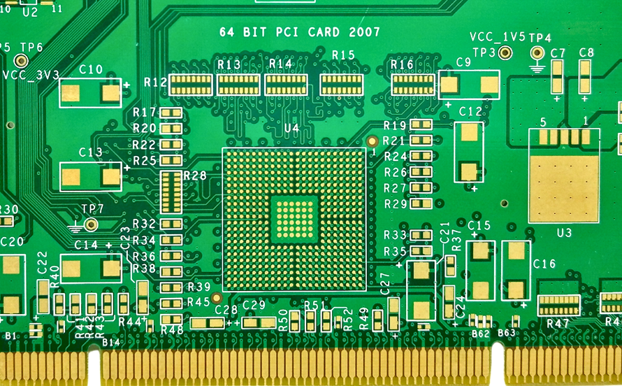
Running out of routing channels after the board is full means going back to placement, which is expensive. Before starting to route, walk along a few critical connections and check whether any corridor is walled off by parts, whether the interfaces can escape cleanly, and whether power and ground have sensible space. Empty area is not automatically wasted area; it is often the condition that lets the design be finished.
Also rehearse real use. Can the programming cable be connected? Can a probe reach the test points you intend to use? Is the polarity marking readable after assembly? Parts that will be hand-soldered or reworked need access that matches their package and the assembly method, and volume production requirements should be confirmed with the assembly, test and mechanical teams rather than assumed from a single generic clearance rule.
Connector Placement and Cable Entry
Connector placement deserves its own pass because it couples the mechanical and electrical worlds. The position is set by the enclosure and the cable route, the pin order is set by the harness, and the copper around it is set by current and signal requirements. Getting the position right but the pin orientation wrong means the harness has to twist or loop, which adds length and often adds noise coupling.
Check the mating direction against the drawing, keep high-current pins away from sensitive analogue pins, and give ground pins a short, wide path to the reference plane. If two connectors share a harness, place them so the cable can be dressed without crossing the board edge. These details cost nothing at placement time and are painful to correct after the outline is committed.
Reading the Rat’s Nest Correctly
The rat’s nest shows connectivity, not quality. A short line does not mean a good connection and a long line does not automatically mean a bad one, because impedance, return path and current density are not visible in it. Use the lines to find the parts that talk to each other most, then apply engineering judgement about which of those conversations are sensitive.
It also helps to sort connections by class: power, ground, high-speed, low-level analogue, and slow control. A board placed to keep the sensitive class short and quiet usually routes much more easily than one placed to minimise the total line length of everything at once.
Common First-Pass Mistakes
Three mistakes show up repeatedly. The first is placing the controller first and treating the edge hardware as an afterthought, which then forces the enclosure interface to move. The second is scattering decoupling capacitors evenly, as if they were decoration, which defeats their purpose. The third is filling every gap, leaving no channel for a bus or a ground pour.
Each mistake has the same root cause: placement decisions made without knowing which constraints are real. A short written list of fixed positions, functional blocks and reserved areas turns placement from an aesthetic exercise into a constraint-solving exercise.
A Workable Review Checklist
Before routing begins, confirm four things. Fixed mechanical positions are marked and respected. Component placement groups follow the connection order of the schematic. Every decoupling group is adjacent to the pins it serves. And the reserved routing, test and assembly space is intact. If any of the four fails, fix it now; see PCB design quality characteristics for how these decisions show up in the finished product.
Route a few of the most critical nets next, even tentatively. If they escape the placement without detours, the layout order did its job. If they do not, the correction is still cheap. It is also worth comparing the mechanical side against board outline and mounting design rules, and checking that the fabrication side of the plan matches PCB manufacturing processes before the file is released.
FAQ
Should I place the biggest chip first? No. Start with the parts whose position is fixed by the enclosure, the mounting hardware and the user interface. The controller is important but its exact location is usually negotiable, which makes it a poor first constraint.
How close do decoupling capacitors need to be? Close enough that the added inductance does not defeat the capacitor, which depends on the device and the frequency of the transient. Follow the datasheet recommendation, keep the loop small, and do not treat the distance as a fixed number for every part.
Is an empty area on the board a mistake? Not necessarily. Space reserved for routing channels, plane integrity, thermal spreading or test access is doing real work. Only unplanned, unusable emptiness is a problem.