Multilayer PCB Manufacturing Challenges: Registration, Lamination and Drilling
A ten layer board is not simply a four layer board with more copper. Every layer added multiplies the number of interfaces that can move relative to one another, and it lengthens the process chain that each panel must survive. Multilayer PCB manufacturing challenges concentrate in four places: registration between layers, the press cycle, drilling through a thick stack, and the reliability physics of thin dielectric layers under bias.
What Makes High Layer Count Boards Different
Boards in the ten to twenty layer range and beyond are built for communication equipment, high-end servers, medical electronics, avionics, industrial control and defence hardware. They combine thick finished board thickness with many layers, dense traces, a high via count, large panel formats and very thin dielectric layers. Each of those properties raises the precision required at every step.
The economic consequence is that scrap costs more. A panel that fails after lamination carries the value of every inner layer already fabricated inside it, and a board that fails at final test carries the whole build. Customer qualification for these products is also long and formal, which is why fabricators guard process stability rather than chasing the tightest possible specification.
Interlayer Registration and the 75 Micrometre Budget
Layer-to-layer alignment is usually held to roughly 75 micrometres for advanced builds, and every source of movement eats into that budget. Large panels expand and contract more than small ones in absolute terms. Cores from different suppliers, or even different lots, behave slightly differently, so their individual growth does not cancel out across a stack.
The alignment method sets the floor. Tooling holes, post-etch punching and optical vision systems achieve different accuracies, and the choice must match the layer count and line width. Imaging rooms are also controlled for temperature and humidity because dimensional movement continues after the artwork has been printed. The fundamentals are covered in our notes on PCB dimensional stability and expansion.
Inner Layer Fabrication on Thin Cores
High layer count designs push toward high Tg, high speed and thick copper laminates with thin dielectric layers. That combination is demanding for inner layer imaging. Line widths and spaces shrink, so opens and shorts both become more likely, and yield falls. Fine-line signal layers also generate more false calls at automated optical inspection, which slows the line and hides real defects among the noise.
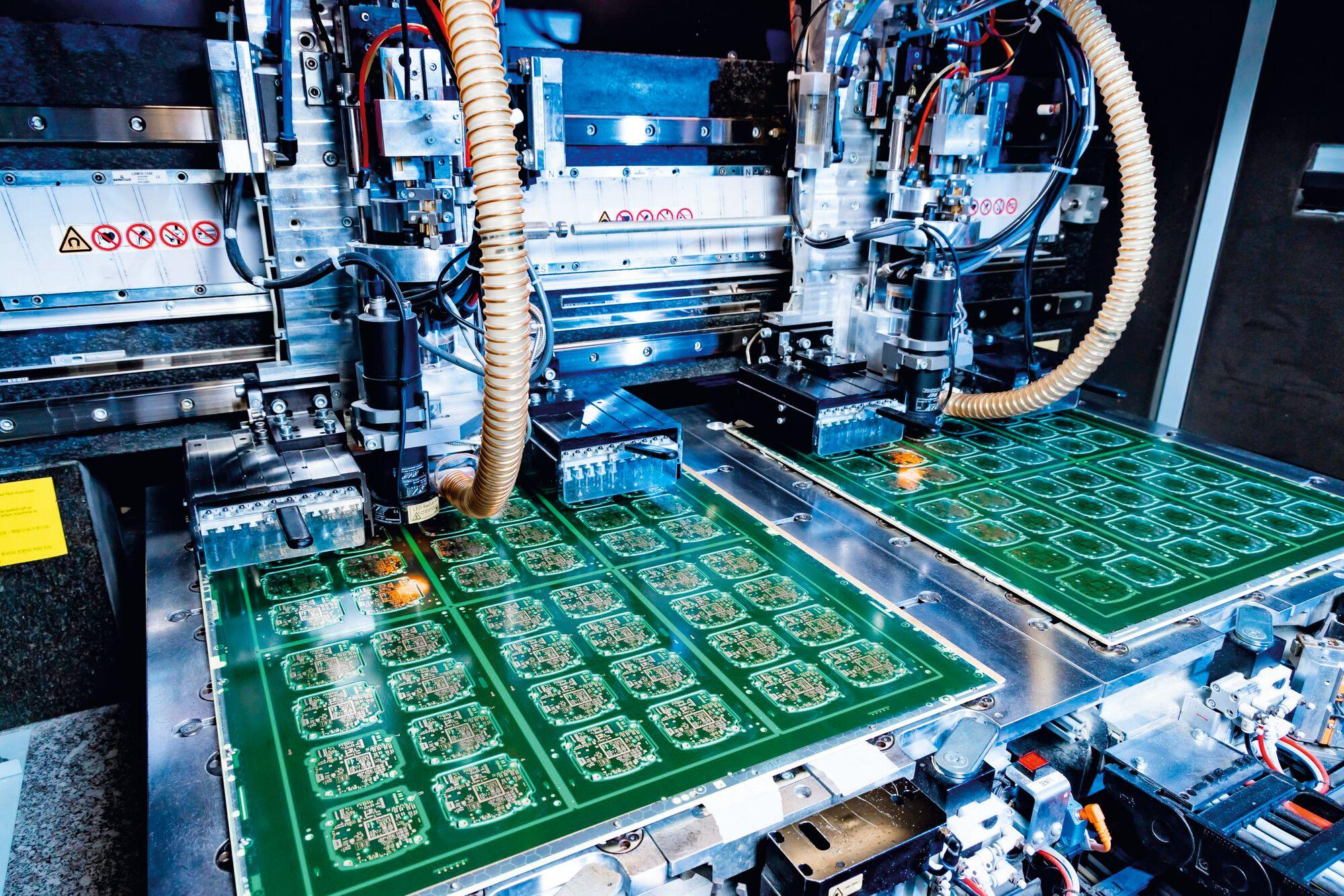
Thin cores bring their own behaviour. They wrinkle during handling, expose poorly when they do not sit flat, and tend to curl as they pass through the etcher. Since these panels are usually large system boards, a single curl-related misregistration can scrap a considerable amount of material. Etch factor must be measured and compensated rather than assumed, and panels should be handled by the edge at every station.
Lamination Defects and the Press Cycle
Lamination stacks many inner cores and prepreg sheets into one bonded unit, and the press cycle is where defects such as slip, delamination, resin voids and trapped air appear. The build must account for the heat resistance of the material, the pressure profile, the resin content of each prepreg and the target dielectric thickness between layers.
Because the stack is thick and asymmetrical heating is unavoidable, expansion and shrinkage compensation cannot be perfectly uniform across all layers. Thin dielectric layers are the first to show the effect, and they often surface as failures during interlayer reliability testing rather than as visible defects. A press recipe built from material data and verified with coupon builds is the only reliable route; the workflow is described in our PCB lamination process guide.
Drilling: Burrs, Desmear and Drill Breakage
High Tg, high speed and thick copper laminates all make drilling harder. They raise hole wall roughness, encourage burrs at the copper interface, and make desmear more aggressive, because more resin smear has to be removed without damaging the dielectric. Every additional layer adds copper to the stack, so the drill has to penetrate more material per hit.
Cumulative copper thickness and finished board thickness are the main causes of drill breakage, and a thick stack also encourages drill deviation from the intended axis. Bit geometry, spindle speed, feed rate, hit count and entry and exit material all have to be tuned per stackup. Dense fine-pitch fields make it worse, because tooling has less room and the consequences of wander are greater.
CAF Risk Where BGA Density Is High
Conductive anodic filament growth is the failure mode that most often decides whether a high layer count design is manufacturable in volume. Under bias and humidity, copper can migrate along the glass-resin interface between two plated holes, eventually bridging them. Narrow hole-to-hole spacing, thin dielectric layers and dense BGA fields all shorten the path the filament has to travel.
Resin chemistry and glass style influence the risk as much as geometry does, and smear left in the hole after drilling accelerates it. The practical response is to respect hole-to-hole spacing rules, validate the laminate system with CAF testing or highly accelerated stress testing, and treat any relaxation of spacing as a change that requires requalification.
Design Choices That Reduce Manufacturing Risk
Most of the risk is set before fabrication begins. A symmetric, balanced stackup keeps the press cycle predictable, avoids excessive thin cores and never places dissimilar laminates in asymmetric positions. Specifying impedance with a sensible tolerance, and leaving the fabricator room to choose prepreg combinations, reduces both cost and the chance of a lamination surprise.

It also helps to plan for the process rather than around it. Include test coupons sized for the qualification programme, keep via-to-copper clearances inside the laminate supplier guidance, and confirm the required reliability standard before the first panel is drilled. Unbalanced builds and their consequences are discussed in balanced stackups and odd layer counts. At gopcb we review stackups against the intended process before release, because fixing registration or lamination problems on paper is far cheaper than fixing them on a panel.
Tooling, Handling and Yield Discipline
Large panel formats are efficient for the fabricator and unforgiving for the process. Panels must be moved on frames or in cassettes rather than by hand, and every station needs edge clearance so that tooling, clamps and conveyor wheels never touch active circuitry. Damage introduced during handling rarely appears as an obvious defect; it shows up later as a registration error or a cracked inner layer.
Yield discipline follows from that. Coupons should sit where they represent the worst case of the build, not in a convenient empty corner, and electrical test should be configured for the full net list rather than a sample. Rework of a high layer count board is limited by the number of reflow cycles the laminate will tolerate, so it is better treated as a scrap decision than a repair opportunity.
FAQ
Why is interlayer registration harder on high layer count boards? Each added layer adds interfaces that can shift, and larger panels amplify the absolute effect of expansion. Registration therefore depends on tooling method, material consistency and imaging room control rather than on a single inspection step.
What causes drill breakage on thick multilayer stacks? The drill must pass through more copper and more board thickness per hit, which raises mechanical load and heat. Wrong feed rate, worn bits or an excessive hit count will snap a tool, and the smaller the hole, the narrower the margin.
When should a design be tested for CAF? Whenever hole-to-hole spacing is tight, dielectric layers are thin, or the product sees continuous bias in humid conditions. Those are the applications where conductive anodic filament growth decides long-term reliability.