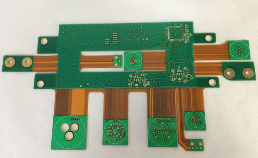
Legend Printing and Solder Mask: How the Process Shapes Design Rules
Solder mask and legend are the two printed layers that most designers treat as decoration, and both of them are process steps with real constraints. The mask has to survive the soldering process and protect the copper; the legend has to remain legible after assembly. Understanding how each is applied explains why some layout choices that look harmless create avoidable defects.
The Mask Sequence in Overview
Before the mask is applied, the copper surface is prepared mechanically, usually by brushing or scrubbing, so that the ink will adhere. The mask is then printed through a screen, with the mesh count chosen according to the ink and the required resolution. After printing, the board is pre-baked to drive off solvent and set the film, then exposed through a photographic tool, developed to remove the unexposed areas over the pads, inspected visually, and finally post-cured to complete the polymerisation.
Each of those steps has parameters that the fabricator controls and that the designer influences indirectly, through the geometry that is being printed.
Screen, Pre-Bake and Cure
The screen mesh determines how much ink is deposited and how fine a feature can be printed. A finer mesh deposits less ink and resolves smaller openings, while a coarser mesh deposits more and covers the copper more reliably. The trade-off becomes visible when the design contains both large planes and fine-pitch pads: the mesh that covers a plane well may not resolve the gap between adjacent pads.
Pre-bake is a drying step, with the temperature and time selected for the ink being used. Too little drying leaves solvent in the film, which causes the mask to flow during exposure or to blister during post-cure. Post-cure completes the cross-linking and determines the final hardness and chemical resistance. Both steps are specified by the ink manufacturer, and a fabricator who shortens either of them to improve throughput produces a mask that looks correct and performs poorly in assembly.

Exposure and Development
Exposure energy determines how completely the mask is cured over the areas that will remain. Under-exposure leaves the mask soft, so that development removes more of it than intended and the mask opening over a pad becomes larger than the artwork specified. Over-exposure produces the opposite problem: the mask closes in, the opening shrinks, and a pad that should be exposed is partially covered, which interferes with solderability.
The development step removes the unexposed mask. The process window has a defined endpoint, and a board that is developed beyond it loses mask from areas that should be covered. Both exposure and development therefore shift the edges of every mask opening, which is why the mask artwork has a defined swell or clearance relative to the copper pad. That clearance is the designer’s responsibility, and it should match the fabricator’s process rather than a default value from a library.

What the Mask Does and Does Not Cover
The mask protects the copper from oxidation and from accidental bridging during soldering, and it also defines where solder can be deposited. It does not provide electrical insulation in the sense of a safety barrier, and it should not be relied on to isolate two conductors at a significant voltage difference. Where isolation is required, the copper spacing has to provide it.
Mask also affects via treatment. A via can be left open, tented with mask over the pad, or plugged and plated over. Each option changes what the assembler can do: a tented via cannot be probed directly, and a via that is left open next to a pad can wick solder away from a joint. The choice should be recorded in the fabrication notes rather than left to chance, and it interacts with the assembly process. Our tented via notes and the mask over via material describe the options.
Legend Printing and Legibility
The legend is printed after the mask, and it is subject to the same geometry limits. A line that is narrower than the process can print reliably will break up, and a character that is too small to resolve will be unreadable precisely where it matters most, next to a fine-pitch device. Most fabricators specify a minimum stroke width and a minimum character height; staying above both is what keeps the legend useful after assembly.
Legibility after assembly is the point of the exercise. Do not place a reference designator where a component body will cover it, and do not place one on a pad. Where the board is dense, moving the designator to a nearby free area, or to an assembly drawing instead of the board, is more useful than shrinking it below the readable limit. Our design release checklist covers the legend review, and the fabrication notes guidance explains how to specify which data layer carries the legend.
Common Mask and Legend Defects
Mask lifted from a copper edge, mask forming a shadow across a pad and legend printed on top of an exposed pad are the defects that appear most often, and all three trace back to geometry. A pad that is too close to a trace leaves no room for the mask to sit between them. A mask opening that is under-sized leaves a ring of mask across the pad. A designator placed inside a pad opening is printed on metal, where it will not adhere.
The remedy is to check the design against the fabrication capability before release, using the same design rule check that verifies copper spacing. Mask and legend rules are frequently left out of a rule set because they are considered cosmetic, which is why the same defects recur in designs from otherwise careful teams.
Specifying the Printed Layers
The mask and legend parameters that the designer controls are the clearance from the copper pad, the minimum stroke width and height of the legend, and the treatment of vias. Each of these should be stated in the fabrication notes rather than inherited from a library default, because the correct value depends on the fabricator’s process. A design that specifies them explicitly can be checked automatically; a design that does not will be adjusted by the fabricator to suit the process, which is a legitimate outcome but not a predictable one.
FAQ
Should the mask opening be larger or smaller than the pad? It should be larger than the copper pad by the fabricator’s specified clearance, so that no mask overlaps the edge of the pad. A mask opening that is the same size as the pad, or smaller, will leave a rim of mask on the pad after normal process variation, and that rim is a common cause of poor soldering on fine-pitch parts.
Can the legend be printed over a solder mask that is over a via? It can, and it is a common way to fill otherwise empty space, but the ink will not adhere to a via that is open. Where the via is tented, the legend prints normally on the mask. Where the via is plugged and plated over, the surface is copper or plating and the legend will not remain, so those areas should be left free of text.
What does gopcb check about mask and legend before fabrication? We check the mask clearance against the copper pads, the minimum legend stroke and character height, the position of designators relative to component bodies, and the handling of vias as tented, open or plugged. These are the parameters that decide whether the printed layers come out as the designer intended, and they are cheapest to correct while the artwork is still being generated.