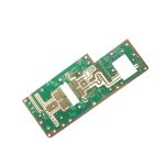
Six Layer PCB Return Path: Stackup and Reference Planes
A signal trace is only half of a circuit. Current leaves the driver, travels along the trace, arrives at the receiver, and must then find its way back to the driver through the reference structure. That second half of the loop is the return path, and on a six layer board it is the part of the design that is easiest to get wrong because it is invisible on the schematic and only appears when a plane is split or a signal changes layer.
What a Return Path Actually Is
The return path is the conductive route that closes the current loop. In a multilayer board that route is normally a ground plane, and the term return layer describes the function that the plane performs rather than a layer with a special name in the stackup. A plane that carries return current is a reference plane, and the same copper may serve as reference for signals on two different layers at once.
At low frequency it is tempting to say that current returns along the path of least resistance. At high frequency the return current is not free to wander: it couples to the signal trace through the field between them, and it concentrates directly beneath the trace, following its every turn. That is why the geometry of the loop, not just the presence of a plane, determines how well a signal behaves and why signal integrity work on a six layer board always starts with the reference structure.
Why the Current Follows the Trace
When a trace runs above a continuous plane, the trace and the plane form a transmission structure. The signal current on the trace and the return current in the plane are separated by the dielectric thickness, and their fields are tightly coupled. The closer the plane is to the trace, the tighter that coupling becomes and the smaller the loop area.
Loop area is the quantity that matters most. A small loop means low inductance, which means less impedance discontinuity and less radiation. It also means the field is confined between trace and plane rather than spreading into the neighbouring region, which reduces coupling into other nets. This is the whole reason a thin dielectric between signal and reference is preferred for fast signals.
<img src="https://www.gopcba.com/wp-content/uploads/2024/09/PCB_test.webp" alt="Six layer stackup showing signal and reference planes” />
Why Six Layers Change the Problem
A four layer board usually offers two signal layers and two plane layers, and the designer has little choice about which signal layer sits next to which reference. A six layer stackup adds freedom, but freedom in the wrong hands produces a stack where a fast signal layer is sandwiched between two other signal layers and refers to a plane that is two dielectric layers away.
On six layers there is also more opportunity to split a plane to accommodate several supply rails. Every split is a barrier to the return current of any fast net that crosses it, and the wider the board the more likely a long route will wander across one. The stackup decision therefore has electrical consequences that are decided long before the routing begins, and the general principles are set out in layer stackup for one to eight layers.
Stackups That Keep the Reference Close
The common six layer arrangement places signal on the outer layers, plane on the inner pair, and signal or plane in the middle, so that every signal layer has a plane within one dielectric thickness. A frequently used version is signal, ground, signal, power, ground, signal, which gives the two outer signal layers an adjacent plane and leaves the middle signal layer with a reference on both sides.
What matters is not the naming of layers but the electrical relationship. Each fast signal layer should be adjacent to a continuous plane, the dielectric between them should be thin enough to give the required impedance, and the plane should be unbroken under the whole route. A stack that satisfies those conditions is a good stack regardless of how its layers are labelled.
What Happens When the Plane Is Split
If a fast signal crosses a gap in its reference plane, the return current cannot follow. It has to detour around the gap, which increases the loop area, raises the inductance of the path, and creates a discontinuity that produces reflection and radiation. In a mixed signal design a crossing of this kind can also inject digital noise directly into an analogue ground region.

The practical rules follow directly. Keep the reference continuous under every fast route, place the crossing point of any unavoidable split away from fast nets, and where a split must be crossed, provide a stitching capacitor or a bridge of vias to carry the return current across. The mechanisms by which these discontinuities become emissions are described in <a href="https://www.gopcba.com/emi-suppression-design-principles/” title=”EMI suppression design principles”>EMI suppression design principles.
Layer Changes and Reference Transitions
A via that takes a signal from one layer to another also moves the return current from one plane to another. If the two planes are at the same potential and are stitched together with vias near the signal via, the return current makes the transition easily. If the reference changes from ground to a power plane, or if the planes are stitched only far away, the return current has to find a longer route and the transition becomes a source of noise.
The standard remedy is a return via placed next to the signal via, or a small capacitor between the two planes if a via is not possible. The same reasoning applies to connectors and to any structure where a fast signal leaves one reference environment and enters another. The interaction between vias and clearance is treated in via to trace clearance in multilayer boards.
Ground and Power Planes as References
A power plane can serve as a reference, and on many boards it must, because there is no room for a dedicated ground plane at every layer. A signal referencing a power plane still has a return path, but the current returns through the power distribution network and its decoupling, which is a higher impedance route than a solid ground plane. That is acceptable for slower signals and less so for the fastest ones.
Where a power plane is used as the reference, the decoupling capacitors between that plane and ground become part of the return path. Their placement and their inductance set how well the reference behaves at high frequency, which is a good reason to treat the power distribution and the reference structure as one design problem rather than two.
Verifying the Design
Verification starts with a visual check of the stackup drawing: for every fast signal layer, identify its reference and confirm that the reference is continuous along the route. A plane check on the layout confirms that no fast net crosses a split, and a via review confirms that each layer change has a return path within a short distance.
Beyond that, the design can be simulated to see the impedance profile along a route and the effect of each transition, and the finished board can be measured. A time domain reflectometry trace that shows a clean impedance indicates that the reference structure is doing its job, while a step in the profile points to the location where the return path was interrupted.
FAQ
Is the return path the same as the ground plane? In most multilayer boards the ground plane carries the return current, but the two ideas are not identical. A power plane, a local reference or a stitched structure can also carry it.
Can a signal cross a split plane safely? It can be made acceptable with a stitching capacitor or a nearby bridge of vias, but the safest answer for a fast net is not to cross at all.
How thin should the dielectric under a fast signal be? Thin enough that the loop area is small and the target impedance is met, which usually means a few tenths of a millimetre on a six layer board.