PCB Design Process: From Netlist to Fabrication Data
A board that is easy to build, easy to test and easy to service is almost always the result of a disciplined PCB design process rather than a clever one. The process produces two things: a layout that satisfies the electrical intent, and a data package that lets a fabricator and an assembly house build it without guessing. When either is missing the cost appears later, as a revision, a rework loop or a batch of boards that cannot be tested.
What the Process Has to Deliver
The electrical requirement arrives as a netlist and a set of constraints: which nets are controlled impedance, which must be matched in length, which carry high current, and which are sensitive. The mechanical requirement arrives as an outline, a height limit and a set of mounting and connector positions. Both are inputs to the layout, and neither can be changed cheaply once routing has begun.
The output is equally specific. Gerbers or an equivalent manufacturing format, a drill file, a stackup drawing, an impedance requirement, a solder mask and paste mask definition, an assembly drawing and a bill of materials that matches the reference designators on the board. A process that delivers all of these consistently is what allows a shop to quote accurately and build to the intended design.
Placement Decides Everything After
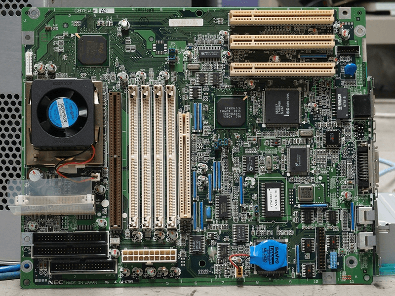
Component placement is where most of the design is decided. Connectors, mounting holes and any part with a mechanical relationship to the enclosure are fixed first, because they cannot move. Then the large devices, the power stage and the clock source are positioned so that the critical connections are short, and only then are the small parts distributed around them.
Two rules pay for themselves immediately. Keep the high current path and the sensitive measurement path apart, so that heat and voltage drop do not reach the analogue circuitry. And place decoupling against the pin it serves rather than in a neat row at the edge of the device, because a capacitor two millimetres away is a capacitor that does nothing at the frequency that matters. Our notes on board outline and mounting design cover the mechanical constraints.
Routing Strategy and Order
Route in order of difficulty, not in order of convenience. Controlled impedance nets, differential pairs, matched length buses and high current paths should be routed while the board is still empty, because they have the least freedom to move. Ordinary digital and low speed analogue nets fill in around them afterwards, and this order avoids the situation where a critical net has to take a long detour around routing that was laid down first.
Keep the reference plane under every signal continuous, and treat a layer change as a decision rather than a detail: a signal that moves reference layers needs a return path, or it becomes a radiating loop. Where the routing is dense, allowing the tool to auto route the easy nets while the critical ones are placed by hand is a legitimate compromise, provided the critical nets are not left to the tool as well.
Planes, Power and Reference
A solid reference plane is the foundation of the layout, and its continuity matters more than its thickness. Splitting a plane forces return currents to detour, and the resulting loop area creates both emissions and sensitivity. Where a split is genuinely needed, it should be placed so that no fast signal crosses the boundary and so that the two regions meet at a single defined point.
Power distribution follows the same logic. A plane pair with thin dielectric between the layers provides a low inductance supply and a useful amount of distributed capacitance, which is why a well built power plane does more for supply integrity than a scatter of capacitors. The current carrying requirement also has to be checked at the narrowest point of the plane, not at its average width. Our notes on PCB design quality characteristics list the checks that matter most.

Design Rule Checks and Review
An automated design rule check catches the mechanical mistakes: clearance violations, unconnected nets, silkscreen over pads, drill sizes outside the process window, and mask slivers that the fabricator cannot produce. The rules themselves have to match the chosen fabricator capability rather than a default library, because a design that passes a generic check may still be outside the process window of the shop that builds it.
Review catches what the tool cannot. Someone other than the author should look at the critical areas: the escape routing from the largest package, the return path under the fastest nets, the thermal path out of the power stage and the placement of the test points. A short review with a written checklist is more effective than a long one without an agenda, and it costs far less than a board revision.
The Fabrication and Assembly Package
The data package should be complete enough that no question needs to be asked. That means a stackup drawing with material and copper weights, an impedance requirement with the coupon geometry, a finish specified per region, a tolerance list and an assembly drawing showing polarity and orientation. Any of these omitted becomes a delay or, worse, a batch of boards built to an assumption.
It should also be readable. Clear layer naming, an unambiguous origin, and a note explaining anything unusual about the board all reduce the chance that a well made board is built to a misunderstanding. Our notes on PCB manufacturing processes and PCBA development show what the receiving shops do with each item.
Common Causes of Rework
Rework usually traces back to one of a small number of causes: pads too small or too close for the assembly process, test points that cannot be probed because a component sits over them, a connector placed where the enclosure will not allow the cable to bend, and a silkscreen reference that does not match the bill of materials. None of these are electrical errors, and all of them are visible in a review.
The remedy is to check the design against the next process rather than only against the schematic. Ask whether the smallest pitch can be printed and placed, whether every net can be reached by a probe or a bed of nails, and whether the board can be removed and refitted inside the enclosure without disturbing the mechanics. Those three questions catch most of the expensive surprises.
Keeping the Process Repeatable
A process is only valuable if it is followed on every project. Written design rules, a standard stackup family, a fixed layer naming convention and a review checklist turn a personal skill into an organisational capability, and they make a new engineer productive far sooner. They also make it possible to compare one project with another when something goes wrong.
Keeping the rules current matters as much as having them. Fabricator capabilities improve, component packages shrink and the interfaces a product must support change, so the rule set should be reviewed periodically and updated with evidence from actual builds rather than with assumptions. Our notes on PCB manufacturing tolerances give a baseline for the process limits.
FAQ
What is the first step in PCB design? Collect the constraints: the netlist, the mechanical outline, the impedance and length requirements, the current paths and the test strategy. Placement follows from those inputs, and a design that starts before they are known will be reworked.
Should routing be done automatically? Auto routing is useful for the ordinary nets on a non critical design. Controlled impedance, matched length, differential and high current nets should be routed by hand, because the tool optimises for completion rather than for electrical behaviour.
What should a fabrication package contain? Gerbers, drill data, a stackup drawing, impedance requirements, a finish and tolerance specification, a paste and mask definition and an assembly drawing. Missing items are the usual cause of delays between release and first article.