High Speed PCB Design for DSP Systems: Noise Control
A DSP runs at high clock rates with fast edges, and a fast edge is what makes a board behave like a transmission line rather than a set of connections. The interference problems that appear in a working system come mostly from three places: the input and output channels, the power supply, and coupling between conductors. Addressing them is a matter of stack-up, placement and routing, taken in that order.
Where Interference Enters a DSP System
The first path is through the input and output channels. In a data acquisition chain, noise on the sensor signal is added to the signal before it is sampled, and the measurement error grows with it. On the output side the same noise can corrupt the data being driven out. Optocouplers and galvanic isolation are the usual answers where the source of the noise is external to the board, because they break the conduction path rather than trying to filter the disturbance out.
The second path is the power supply, which is the largest single source of disturbance in most digital systems. The supply delivers energy and its noise at the same time, which is why decoupling at the point of use is not optional. The third is radiated coupling, in which the field from one conductor induces a current in a neighbouring one. That mechanism has a name, crosstalk, and its strength depends on geometry: how close the conductors are, how long they run in parallel, and how near a return path they have. Spacing signal conductors further apart and bringing them closer to ground reduces it.
Stack-Up for a DSP Board
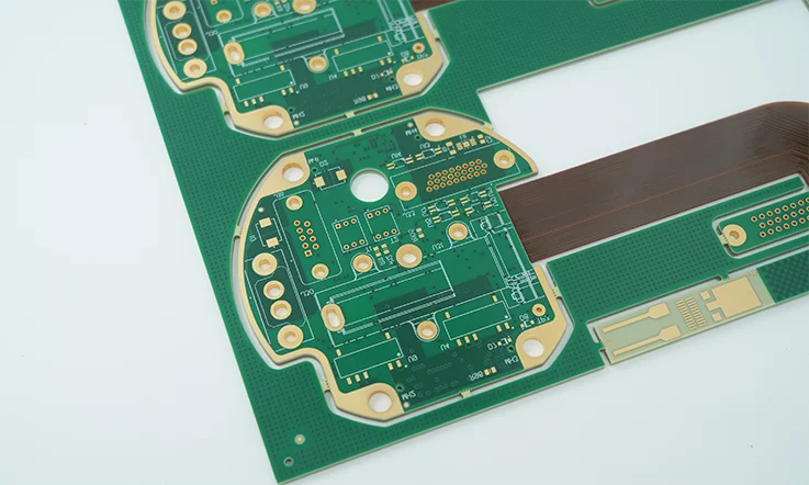
A multilayer stack-up is the normal choice for a DSP board, because it solves several problems at once. It gives every high speed signal a return path directly beneath it, which shortens the loop and reduces the area available for coupling. It allows dedicated power and ground planes, and keeping that pair close together lowers the impedance between them, which suppresses common mode disturbance and keeps supply noise local.
In a typical four layer arrangement the layer beneath the top carries power, so that component supply pins connect without crossing a ground plane, and the critical signals are routed on the bottom layer where there is more room. Keeping all the components on one side is preferable where the design allows it, because a second side of parts adds assembly time and complexity for no electrical benefit; small, cool parts such as chip decoupling capacitors are the reasonable exception when the top side is full. Where the signal count is high, inner layers can carry routing that would otherwise compete for surface space, and blind and buried vias reclaim the area through holes would occupy. How those via structures are chosen is described in blind and buried via stack selection.
Placement Priorities
Placement on a DSP board follows a fixed order. The DSP itself, its program memory, its data memory and any programmable logic go down first, because the routing between them is the densest and the most timing sensitive. Other devices are then placed by function, keeping each function’s components together, and the input and output connectors are placed last, because their position is usually fixed by the enclosure.
Three placements deserve particular attention. The memory devices are the highest speed nets in the system, so the distance between them and the DSP is kept to the minimum the layout allows and the connections are made directly, without detours. Mixed signal devices are separated from the digital section, with the analogue parts grouped so that an analogue ground region can be defined inside the digital ground; where a converter straddles the two, it is treated as an analogue part with a digital return path provided, so that digital noise returns to its own source rather than across the analogue ground. And the clock generator is placed as close to the DSP as possible, with the shortest possible clock trace, kept away from input and output connectors and buses, and with the crystal can grounded.
Decoupling
Decoupling capacitors serve two functions at once. They bypass the high frequency noise a device generates, and they act as a local reservoir that supplies the current the device draws when its outputs switch. Both functions depend on the capacitor being close to the pin, because the inductance of the connection between capacitor and device dominates the impedance at the frequencies involved.
The rule that follows is short and wide. Every supply pin of every large device, including the memory and the programmable logic, gets its own capacitor connected between the supply and ground. The connection from the pad to the capacitor, and from the capacitor to the ground plane, is kept as short and as wide as the layout allows, and it uses generous vias, or several vias in parallel, rather than a single small one. A capacitor that is electrically correct and physically five millimetres away is not doing the job it was placed to do.
Clock and Bus Routing
The clock is the signal most likely to cause trouble, because it switches continuously and its edges are the fastest on the board. The trace is kept short, kept away from connectors and from the input and output wiring, and given a continuous return path beneath it. Where the clock has to reach several devices and the timing budget allows, a matched tree distributes it so that the length from the source to each load is equal.
The data and address buses between the DSP and its memories are the other group that needs attention. They run in parallel over a considerable distance, which is the geometry that produces crosstalk, and their edges are fast enough that the traces behave as transmission lines. Spacing the traces further apart and keeping them close to a ground plane reduces the coupling, and the reasoning behind the spacing rule is set out in the 3W rule for crosstalk. Where the timing budget allows, series termination at the driver damps the reflection that a mismatched line would otherwise produce.
Board Size and Density
Board size is a design decision rather than a given, and both extremes carry a cost. A board that is too large makes every interconnect longer, which raises the impedance of the traces and reduces the noise margin, and it costs more to fabricate. A board that is too small crowds the traces together, leaves no room for heat to escape and increases coupling between adjacent conductors.
The working approach is to select the devices first, calculate the routing space they require, and derive the board size from that rather than choosing a size and fitting the design into it. Where the two conflict, keeping a dense design manufacturable is largely a matter of restraint in routing, and the improvements that cost nothing are described in low cost signal quality improvements.
FAQ
Why does a DSP board need more than two layers? Because a multilayer stack-up gives every high speed signal a return path directly beneath it, and it allows power and ground planes to be placed close together, which lowers the impedance between them.
Where should decoupling capacitors be placed? At the supply pin of the device they serve, with a short and wide connection and adequate vias. The inductance of a long connection dominates the impedance at the frequencies where the capacitor is needed.
How can crosstalk be reduced? By increasing the spacing between parallel conductors, keeping them close to a ground plane, and reducing the distance they run in parallel. The 3W rule is a starting point for the spacing.
Is a smaller board always better? No. A board that is too small crowds the routing, restricts heat removal and increases coupling. The size should follow from the devices and the routing they need.