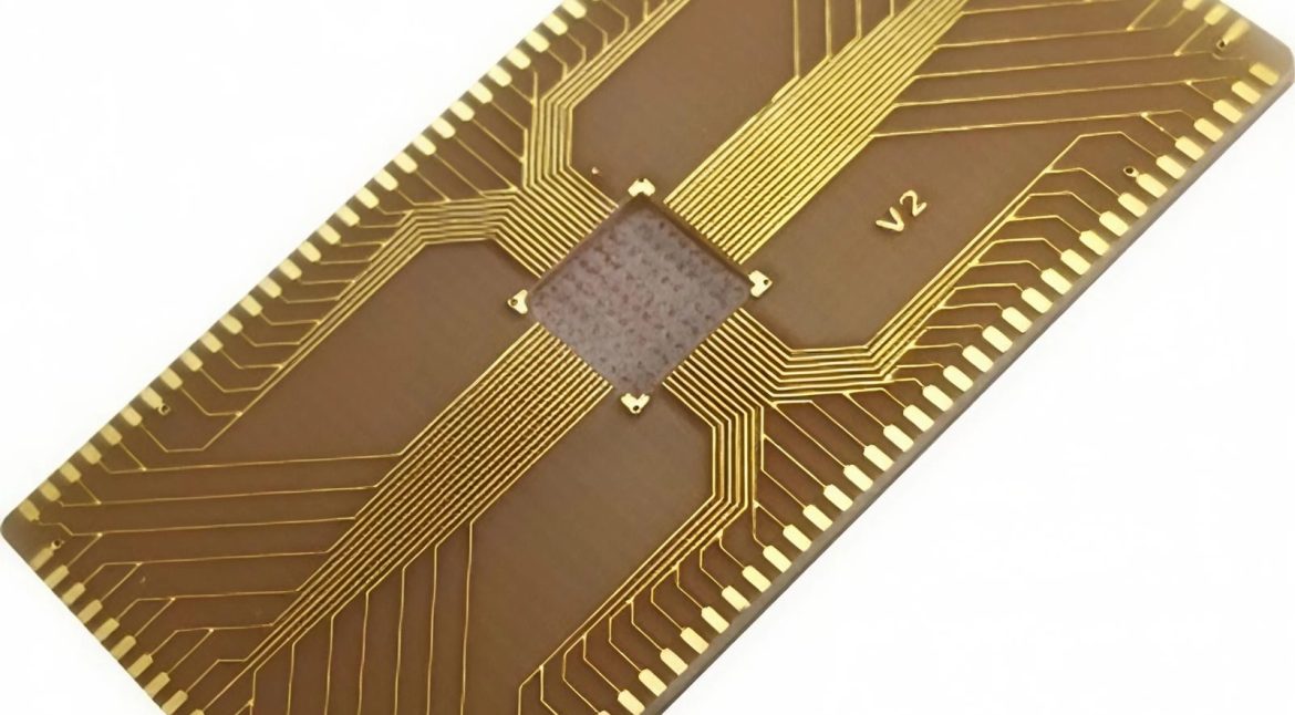
X-Ray Inspection for PCB Fault Detection
As packages have moved from visible leads to hidden solder balls, optical inspection has lost its grip on the most critical joints on the board. A ball grid array hides every connection beneath the package, and a through-hole barrel is buried inside the laminate. X-ray inspection fills that gap by imaging what light cannot reach, and it has become a standard step in any assembly flow that builds boards with BGA, QFN or fine pitch components.
Why Optical Inspection Is Not Enough
Automated optical inspection reads the top surface of the assembly. It catches missing parts, misplaced parts and solder bridges that are visible from above, and it does so quickly. What it cannot see is anything under a package: whether the solder ball actually reflowed, whether two adjacent balls are joined by a hidden bridge, or whether the joint has separated inside the package.
Blind and buried vias in the bare board have the same problem. A plated barrel that cracked during thermal cycling leaves no visible trace on the surface, and the fault appears as an intermittent open that moves when the board flexes. X-ray inspection is often the only non destructive way to find both classes of defect before the product ships.
How X-Ray Imaging Works on a Board
An X-ray source on one side of the board and a detector on the other produce a transmission image in which dense material attenuates more of the beam. Solder and copper are dense compared with the laminate and the package body, so joints appear as bright shapes against a darker background. The contrast between a well formed fillet and a void is usually obvious once the operator knows what to expect at each package type.
Resolution depends on the focal spot of the source and the geometry of the setup. A microfocus tube with high geometric magnification resolves individual balls in a fine pitch array, while a lower magnification view covers the whole panel in one exposure. Most production lines compromise with several magnifications and several angles, because a single straight down view can be ambiguous where joints overlap vertically.
Reading a BGA Image: Voids, Bridging and Head-in-Pillow
In a BGA image each ball should appear as a round, evenly bright disc with a dark halo from the package. Voids appear as dark spots inside the ball, and a small amount of voiding is normal because flux volatiles form bubbles as the solder melts. The defect to look for is a large void or a cluster of them near the pad interface, which reduces the load bearing area of the joint and hurts thermal performance.
Bridging shows as a continuous bright path between two balls that should be separate, and it is usually a stencil or paste volume problem. Head-in-pillow is subtler: the ball and the paste have each reflowed but never merged, leaving a horizontal plane inside the joint that appears as a faint discontinuity. Our notes on SMT process window capability explain why this defect tends to appear on warped packages near the edge of the reflow window.
Voids, Vias and Plated Barrel Defects
A void in a plated barrel is a break in the copper that carries current between layers, and it may not fail until the board has been through many thermal cycles. In an X-ray image the barrel appears as two bright walls with a hollow centre, and a void interrupts one of the walls. Because the defect is inside the material, no amount of external cleaning or rework will reach it, which is why detection at incoming inspection matters so much.
Voiding in thermal pads follows the same principle. A pad that is only seventy percent soldered may pass functional test and still run twenty degrees hotter than a fully soldered one. Quantifying void percentage from the image, rather than judging by eye, gives an objective number that can be compared against a specification, and it is the only way to track improvement over time.
<img src="https://www.gopcba.com/wp-content/uploads/2026/09/233.jpg" alt="Computed tomography slice through a solder joint showing a void” />
Two Dimensional, Oblique and Computed Tomography
A two dimensional image is the fastest and cheapest option and is sufficient for most production screening. Oblique views tilt the sample so that a joint hidden behind another becomes visible, which resolves most of the ambiguity that arises when components sit in a row. Both are quick enough to place at the end of a production line.
Computed tomography reconstructs a three dimensional volume from many projections, which separates features at different heights and makes internal structures unambiguous. It is slower and more expensive, so it is normally reserved for failure analysis, for first article qualification of a new package, and for disputes where the exact geometry of a joint has to be established beyond argument.
Failure Analysis Workflow After a Finding
An X-ray image is evidence, not a diagnosis. When it reveals a defect, the next step is to correlate the finding with the process data for that lot: paste volume from the printer, reflow profile from the oven, and placement accuracy from the mounter. A single voided joint is usually a local disturbance, while a pattern across the panel points at a process that has drifted.
Destructive analysis follows when the mechanism matters. Cross sectioning a joint and examining it under a microscope confirms whether the defect was a void, an oxide layer or a crack, and the distinction changes the corrective action entirely. Our overview of SMT inspection methods describes how X-ray fits alongside optical and electrical test in a complete inspection strategy.
Limits of X-Ray and When It Misleads
X-ray is not a universal answer. It struggles with low density materials, cannot detect a poor wetting angle that is geometrically sound, and produces overlapping shadows wherever the board is dense. A negative X-ray result means the joints that were imaged are free of visible gross defects; it does not prove that the assembly will work.
Interpretation also depends heavily on the operator. Image quality varies with the setup, and a marginal void can be read as acceptable by one technician and as a reject by another. The remedy is a written acceptance specification with reference images, tied into the wider PCB quality control flow so that the standard does not change from shift to shift.
FAQ
What void percentage is acceptable in a BGA joint? The answer depends on the application and the customer specification. Consumer products commonly accept up to twenty five percent, automotive and aerospace requirements are far tighter, and thermal pads are more sensitive than signal balls because the void directly increases thermal resistance. Agree the number in writing before production starts.
Can X-ray inspection find a cracked via? Often, yes, particularly when the crack interrupts the plating across the full barrel width and the imaging resolution is high enough. Partial cracks and microcracks are much harder to detect reliably, which is why bare board testing and thermal cycle qualification remain necessary alongside imaging.
Should X-ray be a sample check or a full inspection? Full inspection is normal for boards with fine pitch BGA and for products where a field failure is expensive. Sampling is defensible for mature processes with good process capability data, but the sample should be taken from every panel position, not from the same convenient corner each time.