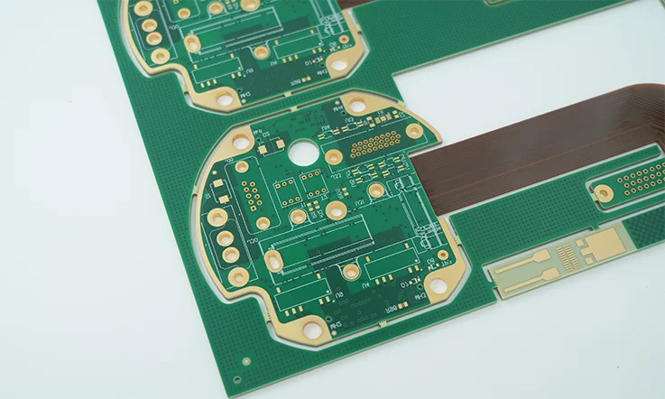
Via Stubs and Via Effects in High Speed Design
A via looks electrically innocent on a schematic, and at low frequency it is. At multi gigabit rates it becomes one of the most significant discontinuities on the board, because the plated barrel is a capacitor, the unused portion below the trace is a stub, and the return path is broken by the very hole that carries the signal. Understanding what a via does to a channel is the difference between a link with margin and one that fails intermittently at temperature.
What a Via Adds to a Trace
The barrel and its pads add capacitance to the line, and the capacitance increases with the pad diameter and with the antipad clearance in the reference planes. That extra capacitance lowers the local impedance, so the signal sees a dip rather than a smooth continuation, and part of the wave reflects back toward the source. The effect is proportional to the capacitance and to the edge rate of the signal passing through it.
The via also adds inductance, which comes from the length of the barrel and from the geometry of the current path through it. In a thick backplane the barrel can be several millimetres long, and the inductance that represents is enough to matter on its own. Our notes on impedance discontinuity analysis show how both effects appear in a measured time domain profile.
<img src="https://www.gopcba.com/wp-content/uploads/2025/05/DIP拉线风彩.jpg" alt="Cross section of a via stub below a signal layer” />
The Stub and Its Resonance
A via is normally drilled through the whole board, so the portion of the barrel below the layer where the signal enters carries no signal. That unused section behaves as a resonant stub, and at the frequency where its length equals a quarter wavelength it presents a short circuit to the line. The result is a sharp notch in the insertion loss and a corresponding peak in the return loss, and it is deep enough to close a channel.
The resonance frequency depends on the stub length and on the effective dielectric constant around it, so a shorter stub pushes the notch higher. On a thick board, or where a signal enters a via near the top and must travel to an inner layer, the stub can easily be long enough to place the notch inside the band the link needs. That is why the layer a signal uses, and where in the stackup it enters a via, becomes a routing decision rather than an arbitrary choice.
Back Drilling and Its Limits
Back drilling removes the unused portion of the barrel after plating by re-drilling the hole to a controlled depth with a slightly larger bit. The stub is shortened dramatically, the resonance moves well above the band of interest, and the channel gains margin. It is the standard remedy on thick, high speed backplanes and on any design where via stubs cannot be avoided by layer assignment.
The process has practical limits. Drilling depth has a tolerance, so a residual stub always remains and must be included in the model. The larger drill also consumes space around the via, which affects routing density, and the operation adds cost and lead time. Where the design allows, moving the signal to a layer closer to the far side of the board achieves a similar reduction without any extra process step. Our notes on back drilling design cover the depth and tolerance considerations.
Return Vias and Reference Changes
When a signal via passes from one layer to another, the return current has to change layers as well, and it needs a path to do so. If the reference planes are stitched by a ground via placed close to the signal via, the return current follows through that via and the loop stays small. Without it, the return current has to find the nearest stitching via on its own, and the loop it travels becomes the dominant discontinuity in the channel.
The same argument applies to a via that changes the reference plane it is referenced to. If the signal moves from a layer referenced to one plane to a layer referenced to another, and those planes are not connected close by, the return current has no short path and the impedance seen by the signal changes abruptly. Placing a stitching via adjacent to every signal via, and a pair of vias where the reference changes, is the standard mitigation.
Via Design Rules for High Speed Nets
Several geometry choices reduce the via discontinuity without any extra process. Keep the pad and antipad as small as the manufacturing tolerance allows, because both add capacitance. Use the shortest possible barrel by choosing layers carefully, so that the stub is short even without back drilling. Where a differential pair changes layer, place the two vias symmetrically and keep the spacing consistent so that the pair does not become unbalanced.
Then confirm the numbers. Ask the fabricator for the actual finished hole size and pad diameter, because the capacitance depends on them, and model the via with those values rather than with nominal ones. On a channel that is marginal, replacing a through via with a blind or buried via in a high density build can remove the stub entirely, at the cost of a more expensive substrate. Our notes on via plugging and microstrip and stripline routing describe the related fabrication and routing options.
Simulating and Measuring a Via
A via is small enough that a full wave field solver is the appropriate tool, and most high speed designs model the critical vias explicitly rather than relying on a lumped estimate. The model needs the pad diameter, the antipad, the stub length, the plating thickness and the dielectric properties, and where those values are uncertain the result is only as good as the least certain input.
Measurement closes the loop. A time domain reflectometer trace through a coupon that includes the same via geometry shows the dip and the following recovery, and a frequency domain measurement shows the stub notch directly. Comparing the two with the model identifies which parameter was wrong, and the answer is usually the stub length or the dielectric constant rather than anything more exotic.
FAQ
Can a via stub really break a link? It can. A long stub places a resonant notch inside the band, and if that notch coincides with a significant portion of the signal spectrum the channel loses margin. Shortening the stub or back drilling moves the notch out of the way.
Is back drilling always necessary on thick boards? No. It is used when the stub is long enough to matter at the operating rate. Careful layer assignment, placing the signal close to the far side of the board, can reduce the stub enough to make the extra process unnecessary.
How many return vias does a signal via need? One placed immediately adjacent is the minimum and is usually sufficient for a single ended net. Differential pairs benefit from a return via on each side, and the spacing should mirror the pair geometry.
Keeping a record of via effects across a project is worth the effort. When a channel fails, comparing the geometry of the vias on that link with one that works usually identifies the difference immediately, whether it is a longer stub, a larger pad or a missing return via. Documenting the parameters on the fabrication drawing, rather than leaving them to the default library, keeps that comparison meaningful.