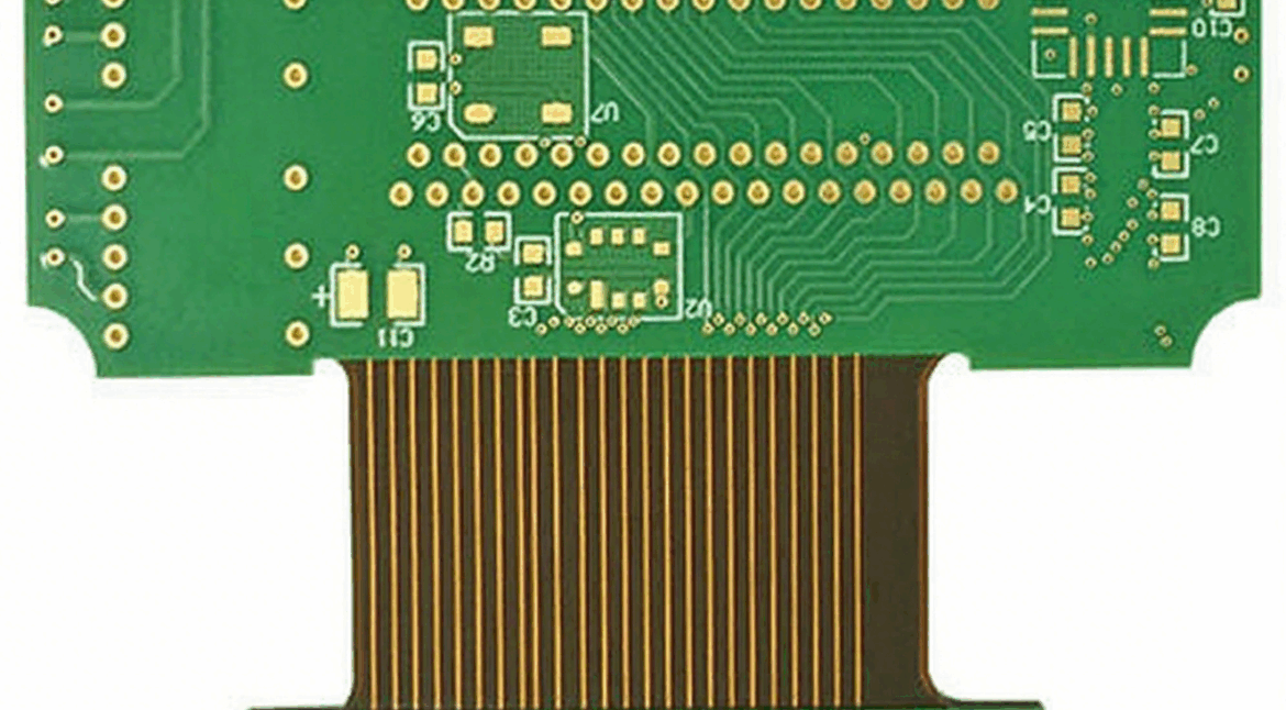
Computer PCB Price Guide: Motherboard, GPU and Server Boards
Almost every product with a processor contains a computer board, and the price range across that family is enormous. A simple control board with two layers and a microcontroller sits at the bottom, while a server motherboard with twelve layers and a dense backplane interface sits two orders of magnitude above it. Understanding a computer PCB price therefore means understanding which class of product is being built, because the cost structure changes completely between them.
What Drives a Computer PCB Price
Four things set the base rate: layer count, material, copper weight and the precision of the pattern. Layer count determines how many lamination and imaging cycles the panel goes through, material determines the dielectric cost, copper weight decides how much metal is plated, and pattern precision decides the yield. A price without those four parameters attached is not a quotation, it is a starting point.
Quantity then changes how the fixed portion is spread. Engineering, CAM work, tooling, impedance verification and test development are charged once, so a five-piece prototype order carries them entirely while a thousand-piece order divides them into fractions of a cent. Comparing quotes at different quantities is the most common mistake in sizing conductors for current driven cost estimates and in procurement generally.
Layer Count by Product Class
Precision is the parameter that is easiest to overlook. Minimum line width, minimum annular ring and the tolerance on every drilled hole all affect yield, and yield is exactly what the fabricator prices. A design that keeps its finest features on the inner layers and uses relaxed geometry on the outer layers is easier to build than one that pushes the limits everywhere, and it usually reaches the same electrical result for less money.
Basic control boards use two layers with one routed side, and they are priced by area rather than by complexity. Entry-level motherboards and memory modules move to four layers, where one internal layer becomes a ground plane and the other carries the supply split. That change roughly doubles the fabrication price but it also makes the board work reliably.
Performance products keep climbing. A graphics board typically uses six to eight layers because it needs several power planes and a wide memory bus, and a server or workstation board can reach ten or twelve layers with a thick backplane structure. At that point an eight layer stackup is not a luxury but the minimum that can support the routing and the return paths.
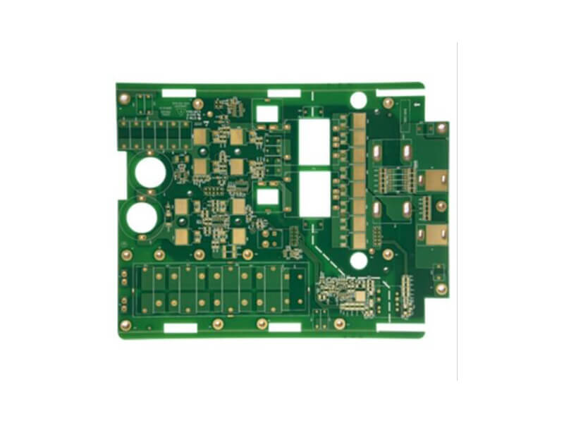
Materials: Standard FR-4, High-Tg and Low-Loss
Standard FR-4 serves two and four layer boards well, but it degrades as layer count and signal speed rise. High-Tg FR4 costs more and holds its dimensions better through repeated reflow, which is important when a thick board is assembled twice. It also reduces the risk of barrel cracking in a board that has many through-holes and a large thermal mass.
Low-loss laminate is the next step and it is priced very differently, because the resin chemistry rather than the glass fabric dominates the cost. It is specified when insertion loss or phase stability actually matter, which on a computer board usually means the memory bus and the high-speed serial links rather than the whole design. A mixed stackup keeps those layers on low-loss material and the rest on FR-4.
Copper Weight, Thickness and Power Delivery
Copper weight is a whole-board cost even when only one net carries heavy current. A processor core rail might need two or three ounces of copper on an inner plane, and once the plane is defined the material is bought for the entire panel. The alternative is to keep the plane thin and add copper area, which is cheaper but consumes routing space.
Finished thickness interacts with the same decision. A 1.6 mm board is standard, and going thicker adds material and reduces the number of panels per stack. On a board with a large connector array the thickness is usually fixed by the connector, so the stackup has to be designed around it rather than chosen freely.

Surface Finish and Impedance Control
HASL is the cheapest finish and is adequate when the finest pitch on the board is generous. ENIG gives a flat surface for fine-pitch packages and multiple reflow passes, which is why performance boards almost always use it. Beyond the finish, an HDI structure with laser vias and stacked microvias adds sequential lamination and drives the price up sharply.
Impedance control is a separate line item in most quotations. It requires a defined stackup, controlled dielectric thickness, test coupons on the panel and a measurement step. On a memory or graphics interface it is unavoidable, but specifying it on nets that do not need it adds cost and engineering time without improving the product.
Prototype versus Volume Pricing
The pcb prototype cost of a complex computer board is dominated by engineering rather than by material. A first build includes a stencil, a test programme, an impedance check, a microsection to verify the stackup and often a first-article inspection report. On a small order those charges can exceed the board cost itself, which is normal and should be planned for.
Volume pricing then depends on yield rather than on the material rate. A twelve-layer board with fine lines and a dense via field will always have a lower yield than a four-layer board, and the fabricator will price that expectation into the unit rate. Improving the design for manufacturability is therefore one of the most effective cost reductions available at this layer count.
Regional Pricing and Hidden Costs
Regional gaps are widest on simple boards and narrowest on advanced ones, because material and process time dominate the price at high layer counts. What remains is yield, inspection depth and documentation rather than labour. Freight and duty then apply to a higher declared value, so the landed cost can differ more than the ex-works rate suggests.
Hidden costs cluster around tooling and verification. CAM engineering, impedance coupons, flying probe or fixture test, X-ray inspection of fine-pitch packages and expedited handling are frequently quoted separately, and a design change after tooling is ordered adds blind and buried via and drilling programmes again.
Reducing Cost Without Losing Signal Integrity
It is worth asking for the quotation to be itemised rather than aggregated, because the two groups of cost respond differently to negotiation. Engineering and tooling are often negotiable on a first order or absorbed against a volume commitment, while material and process time are not. Knowing which is which stops a buyer from spending commercial leverage on the part of the price that cannot move at all.
The largest savings come from restraint. Keep the layer count at the minimum the routing genuinely needs, use low-loss material only on the layers that carry the fastest links, and avoid an HDI structure unless the escape routing cannot be completed mechanically. Each of those decisions removes a process step rather than a feature.
Panel design is the second lever. A board outline that nests efficiently, a standard finished thickness and a stackup that can be built without sequential lamination all reduce cost without touching the circuit. Order size is the third, and the fall between a few hundred and a few thousand pieces is the single largest reduction a buyer can influence directly.
FAQ
How many layers does a motherboard need? Most entry-level boards work on four layers, mainstream products use six, and performance or server boards use eight to twelve with several power planes. The driver is the memory bus and the number of independent supply rails, not the processor itself.
Is low-loss material needed everywhere? No. It is normally used only on the layers that carry the fastest links. A mixed stackup keeps the cost of the remaining layers at FR-4 rates and still gives the loss performance where it is required.
Why is impedance control quoted separately? It requires a defined stackup, controlled dielectric thickness, test coupons and a measurement step, all of which are additional work for the fabricator. It is worth paying for on high-speed nets and unnecessary on slow control signals.