High Density Layout: Escape Routing and Fanout for Dense Boards
Density is what forces a layout to become clever. When a device has more pins than the space around it can escape, the routing must go through the board rather than around the package, and every decision about vias, layers and channel widths suddenly has a cost. A high density layout is not simply a small board; it is a board where the escape strategy was planned before the first trace was drawn, and where the layer stack exists to serve that strategy.
Start With the Escape, Not the Netlist
Escape routing is the process of getting every signal out from under a fine pitch package to the rest of the board. The number of traces that can leave a row of pads per layer is limited by the pad pitch and the trace width and spacing, so the count of layers needed is largely determined by the package before any other routing is considered.
Working out that arithmetic first prevents the common failure where a layout is half finished before the designer discovers that the escape needs more layers than the stack provides. Counting the traces that must leave each side of the package, dividing by the number that fit per layer, and multiplying by the number of rows gives a realistic figure for the escape layers required. Our notes on high density interconnect describe how the stackup supports it.
Fanout Strategy and Via Choices
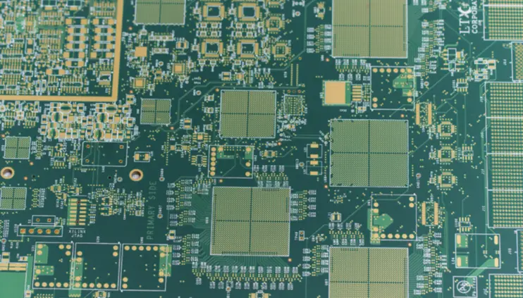
Fanout is the pattern used to bring each pad out, and the choice affects everything downstream. A dog bone fanout places a via beside the pad and routes a short trace to it, which needs space between pads and works well where the pitch allows. Where the pitch does not allow it, the via must go under the pad itself, which is via in pad and requires filling and capping so that the pad remains flat for assembly.
Microvias change the arithmetic in the designers favour. Because a laser drilled via is much smaller than a mechanically drilled one, more of them fit between pads, and an any layer structure allows a via wherever the routing needs one rather than only on a drilled core. The cost is a more expensive substrate and a narrower process window, which is why the decision should be made from the escape count rather than from a preference. Our notes on any layer HDI and via plugging cover the fabrication side.
Routing Channels and Layer Planning
A routing channel is the space between two rows of pads or two components available for traces. Its width in trace pitches determines how much signal can pass, and on a dense board the channels are the scarce resource. Planning them as part of the placement, rather than discovering them during routing, is what separates a layout that closes from one that needs another revision.
Layer planning follows. Signals should be assigned to layers so that each has a reference plane and so that the longest runs sit on the inner layers where impedance is best controlled. Power and ground need enough plane area and enough vias to carry their current, and the planes must remain continuous under the dense routing rather than being carved up by the escape. Our notes on PCB routing rules set out the constraints.
Trace Widths, Spacing and the Cost of Density
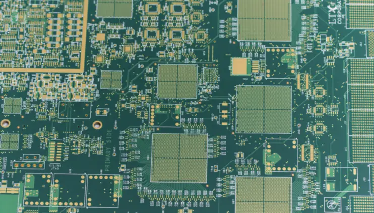
Density forces narrow traces and tight spacing, and both have consequences. A narrower trace has more resistance and, on a controlled impedance net, requires a thinner dielectric to reach the same impedance. Tight spacing increases crosstalk, which on a dense board is often the limiting factor rather than the impedance itself. The usual relief is to make the dielectric thinner, which contains the field and reduces coupling as well as correcting the impedance.
The cost of that relief is mechanical. Thinner dielectrics make the board harder to build, reduce its stiffness and can worsen warpage unless the copper is balanced across the layers. On a high density design the stackup is therefore a negotiated compromise between electrical performance and manufacturability, and it is worth discussing with the fabricator before the layer count is frozen rather than afterwards.
Thermal and Mechanical Constraints in a Dense Board
A dense board has less copper available for heat spreading, because the routing and the vias have removed much of the plane area. The same density that makes the board attractive electrically makes it harder to cool, so the thermal path has to be planned as explicitly as the routing. Thermal vias under power devices, copper on the opposite side of the board and a defined connection to the chassis all become part of the layer plan.
Mechanically, a dense board is thinner and more flexible than a sparse one, which affects handling and assembly. Stiffeners, thicker cores in the stackup or an additional plane can restore rigidity where a large connector or a heavy component is mounted. Our notes on PCB thermal design rules cover the trade-offs in more detail.
Verification Before Release
Rules that matter on a dense board are specific: the minimum annular ring after registration, the drill to copper clearance, the aspect ratio of the deepest via, and the registration tolerance between layers. These should be confirmed with the fabricator rather than assumed, because a design that exceeds the process limits will be built with reduced yield or rejected at the design for manufacture stage.
The final check is the escape itself. Verify that every pad has a legal connection, that no via is closer to another than the process allows, and that the plane under the dense area is still continuous enough to give the signals a return path. On a high density layout, these three checks catch most of the defects that would otherwise appear as opens, shorts or emissions. Our notes on PCB manufacturing tolerances give the numbers to check against.
Why the Strategy Belongs in the Placement
The escape strategy and the placement are the same decision made from two directions. Where the large package sits on the board determines which sides have room to fan out and how long the escape traces must be, and moving it by a few millimetres can change the number of layers required. Positioning the package to give the densest side the most room is one of the highest value decisions on a dense design.
The same applies to the parts that must connect to it. Memory, power devices and connectors all have preferred positions relative to the package, and placing them so that their connections use the escape channels rather than competing for them is what keeps the layout closable. Treating the escape plan and the placement plan as one exercise, rather than placing first and routing second, is the discipline that a high density board demands.
FAQ
How do I know how many layers a dense board needs? Count the traces that must escape from the largest package, divide by the number that fit per layer for the chosen pitch and width, and allow for plane pairs. The escape requirement usually sets the minimum.
Is via in pad always required on a dense board? Only where the pitch does not leave room for a via beside the pad. Where it is used, the via must be filled and capped so that the pad stays flat for assembly.
Does density make a board harder to cool? Usually, because less copper area is left for spreading. The thermal path then has to be designed deliberately, using copper on both sides, thermal vias and a defined route into the enclosure.