
Unintended Capacitance and Coupling in a PCB Layout
Every pair of conductors on a board has capacitance between them, whether the designer intended it or not. Most of the time the value is small enough to ignore; when it is not, the effect appears as a slower edge, a coupled pulse on a neighbouring net or a supply that consumes more current than the calculation predicted.
This article looks at where unintended capacitance and coupling come from in a layout, how they show themselves, and which of the design rules exist to keep them under control.
Where Unintended Capacitance Comes From
Capacitance depends on area, separation and the material between the conductors, and a board offers all three in abundance. Two traces that run side by side on the same layer form one capacitor, a trace passing over a plane forms another, and a trace that crosses a plane boundary forms a third, different from the others because the return path is no longer directly beneath it.
None of these is a fault in itself. The problem arises when the capacitance is large enough to change the timing of a signal, or when it provides a path along which energy travels from a net that switches to a net that measures.
Planes as Both Shield and Capacitor
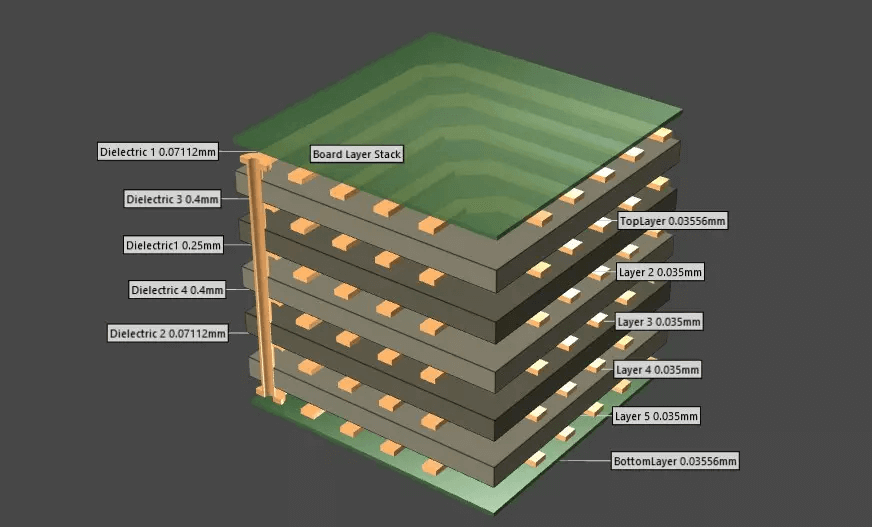
A ground plane is usually described as a shield, and it does reduce the coupling between the layers above and below it, because the field from a trace terminates on the copper rather than reaching the far side. The same copper, however, forms capacitance with every trace that runs past it.
The effect is strongest where a large area of copper sits close to a layer carrying fast signals, because the capacitance per unit length is high and the trace is long. The trade-off is managed through the stack-up: the plane is kept, because the return path and the shielding are worth more than the capacitance costs, and the dielectric height under the fastest nets is chosen with both effects in view.
Coupling Between Traces: Length and Angle
Coupling between two traces grows with the length over which they run parallel and with the speed of the edges involved. Two nets routed side by side for ten millimetres as they approach a connector couple far more than the same two nets crossing at an angle.
The remedies are structural rather than electrical. The length of the parallel run is reduced where the interface allows, the spacing is increased where it does not, and a grounded trace between the two acts as a barrier. Where two layers must both carry routing, the traces on one are run across the other at an angle rather than alongside, because parallel traces on adjacent layers couple through the dielectric, which is a second coupling path that spacing on one layer alone cannot fix. The <a href="https://www.gopcba.com/crosstalk-3w-rule/” title=”spacing rules used to limit crosstalk”>spacing rules used to limit crosstalk describe the usual compromise.
Loops, Stubs and Sharp Bends
A current always returns to its source, and the area enclosed by the path it takes is what radiates and what picks up interference. A trace whose return path is far away encloses a large return loop; a trace whose return is directly beneath it encloses almost nothing.
Stubs and sharp bends add to the problem in smaller ways. A short spur left on a net behaves as a small antenna and as a resonator at some frequency, and a right-angle bend changes the width of the conductor at the corner, which is a discontinuity in impedance. Both are visible in the layout and both are cheap to remove, and neither shows up in a schematic. The mechanisms behind the emissions they cause are set out in the principles of interference suppression.

Vias and the Cost of Layer Changes
A via is a discontinuity. The hole removes copper from the plane it passes through, the barrel adds inductance in series with the signal, and the unused portion of the barrel below the layer where the signal leaves is a stub. On a fast net, several of these changes along one route accumulate into something the receiver notices.
The practical rules follow from that. A signal changes layers as few times as possible, each change is accompanied by a return via so that the return path follows the signal, and vias are kept clear of the reference plane openings that they create. The geometry is described in the via design rules, and the reason a designer should care is that a via is usually the largest single discontinuity on an otherwise uniform line.
Parasitic Capacitance and the Design Rule Check
The design rule check is the tool that finds the unintended capacitance and coupling that a designer cannot see on a screen. It reports traces that are closer than the rule allows, parallel runs that exceed the permitted length, and areas where the return path is broken.
What it cannot do is decide which of the reported items matter. A violation on a slow net that carries no sensitive measurement may be harmless, while one on a clock line may be the cause of a failure that appears only at temperature. Reading the report with the critical nets in mind is what turns it from a list into a decision, and the arrangement of the ground and power conductors is usually where the important answers lie.
Standardisation and Templates
Many of the problems described here have been solved before, in the same form, on a previous project. A template that carries the proven stack-up, the standard via sizes, the rule set and the standard decoupling pattern removes the need to solve them again, and it removes the variation that appears when two designers start from nothing.
A template is not a substitute for thought, because the requirements of a new product differ. It is a starting point that has already eliminated the ordinary mistakes, leaving the designer free to spend the attention on the parts of the problem that are genuinely new.
Closing the Loop
Unintended capacitance and coupling are found in two places: in the design rule check, which reports the geometry, and in the laboratory, where the symptom appears as a marginal timing margin or an emission above the limit. The value of the layout rules is that they move most of that discovery back to the screen.
Where a problem does escape to the laboratory, the response is worth recording. A note that a particular net needs to be routed over a continuous plane, or that a specific pair must be separated, becomes part of the mixed-signal practice that the next design inherits, and that is how a rule set becomes specific to a company rather than general.
FAQ
Can parasitic capacitance actually be measured on a board? Its effects can be, through the timing and the current consumption of a circuit. The capacitance itself is calculated from the geometry.
Is a ground plane ever a mistake? Not usually, but it has to be placed with the layers it serves in mind. A plane adjacent to a sensitive layer with a very thin dielectric is a capacitor as well as a shield.
How long a parallel run is acceptable? It depends on the edge rate of the aggressor and the sensitivity of the victim. The rule sets a number for the general case, and the critical nets are treated individually.