Practical Notes on LCD TV PCB
Television hardware looks simple from the outside and is dense on the inside. A modern set combines a power supply, a video processor, several high-speed input interfaces and a panel driver, and most of them share a single board. LCD TV PCB assembly therefore has to solve a thermal problem, a signal integrity problem and a soldering problem at the same time.
Board Architecture
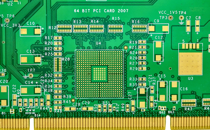
Television main boards are almost always multilayer. The combination of multiple input sources, a high-current power section and a display interface cannot be routed on two layers with an acceptable return path, and the electromagnetic environment inside a television enclosure is hostile enough that a continuous reference plane is a practical necessity.
A four-layer board is the common minimum, with a ground plane and a power plane separating the outer signal layers. Larger sets and higher refresh rates push towards six layers, because the additional inner layers allow the high-speed video signals to be routed with a solid reference on both sides and the power section to be isolated from the processor area.
Material and Stackup Choice
Standard FR-4 is adequate for the digital portion, and it is used for the overwhelming majority of television boards because it is inexpensive, well understood and easy to process in volume. High-frequency laminates are reserved for the radio and tuner sections, where loss and phase stability matter more than material cost.
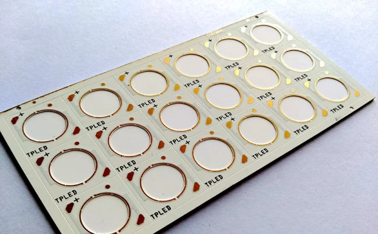
Thermal requirements can push part of the assembly onto a metal-backed substrate. Boards that carry a dense array of light-emitting diodes or a high-power supply stage sometimes use that construction for the thermal section alone, bonded or mounted alongside the FR-4 main board rather than replacing it.
Design Priorities
Power management comes first because it determines the constraints everything else inherits. Regulators must deliver stable voltages under fast load transients, and the copper carrying those currents has to be wide enough that both resistive drop and local heating stay within budget. Decoupling belongs at the pin, not at the far end of the board.
Signal integrity follows. The high-speed inputs carry multi-gigabit data, so the general rules for routing high-frequency traces and data buses apply directly: consistent impedance, short paths, matched differential pairs and a reference plane that is never interrupted under the trace. Grounding and shielding complete the picture, because the display interface and the switching supply are both significant noise sources.
Key Components and Their Constraints
The video processor and microcontroller generate most of the heat on the board and most of the high-speed signals. Their placement therefore drives both the thermal design and the routing plan, and they should be positioned with their memory and their input connectors in mind rather than in the middle of the available area.
The power supply unit carries the largest currents and produces the largest switching noise. Display driver circuitry and the panel interface have strict timing requirements and are sensitive to supply ripple. Passives throughout the board provide voltage stability and noise suppression, and their placement is often what separates a design that passes emissions from one that does not.
Surface Mount Assembly
Assembly of a television board begins with solder paste printing through a stainless steel stencil. Paste volume is the most important single variable in the process, because too little produces an open joint and too much produces bridging. Three-dimensional paste inspection catches the problem before reflow, which is considerably cheaper than catching it afterwards.
Placement follows, with a high-speed machine positioning components and a second machine handling the fine-pitch parts. Reflow then melts the paste and forms the joints, with a profile that has to match the flux chemistry and the thermal mass of a large board. The process steps and their failure modes are covered in more detail in the notes on what causes components to shift during reflow.
Through-Hole and Wave Soldering
Not every part can be surface mounted. Power sockets, large electrolytic capacitors and connectors that must withstand mechanical load are usually through-hole, and they are assembled after the surface mount stage. Those parts are inserted and then soldered by passing the board across a wave of molten solder.
Lead-free versus leaded solder is settled for most production now, but the alloy choice still affects the profile and the appearance of the joint. Lead-free alloys run hotter and wet differently, so the process window for a large board with heavy thermal mass is narrower than it was with tin-lead.
Inspection and Test
Automated optical inspection examines the board for missing, misplaced and tombstoned components, insufficient solder and bridges, using cameras and image processing rather than human judgement. X-ray inspection follows where ball grid array packages or other hidden joints are present, because no optical system can see underneath them.
Electrical test then confirms that the assembly behaves as designed, and a burn-in test runs the board under load at elevated temperature to expose marginal joints and components that would otherwise fail in the field. For a consumer product with a long warranty, that screening is usually cheaper than the returns it prevents.
Common Problems and Their Fixes
Solder defects are the most common, and most of them trace back to the temperature profile or to paste volume rather than to the alloy. Thermal problems come next, and they are usually solved by spreading copper, adding thermal vias under the hottest parts and improving the coupling to the chassis.
Electromagnetic interference is addressed through grounding and shielding, with attention to the interfaces that leave the enclosure. Moisture is a slower failure, and it is handled by a conformal coating that protects the surface without trapping contaminants underneath it.
Where the Technology Is Going
Flexible and rigid-flex constructions are appearing where a set needs a board that folds into a thin enclosure, and high-density interconnect allows more function in the same footprint. Automated inspection with machine learning continues to improve defect detection rates, and lead-free processes are now standard rather than transitional.
Testing is evolving in parallel. In-circuit test and flying probe remain the workhorses for manufacturing faults, while burn-in has become more targeted, focusing on the components and joints that the process data identifies as risky rather than screening everything equally.
Documentation and Handover
Assembly instructions travel with the board rather than living at the factory. Clear reference designators on the silkscreen, a placement file that matches the current revision and a bill of materials with approved alternatives all reduce the chance of a build that is technically correct but functionally wrong. None of it costs more than a few minutes of documentation, and all of it prevents a day of correspondence.
FAQ
Why do television boards need more than four layers? Large panels and high refresh rates raise the number of high-speed channels, and each one needs a clean reference. Six layers allow the video signals to route on inner layers with planes on both sides, which four layers cannot always provide.
Is wave soldering still used for televisions? Yes, for through-hole connectors and power components. Selective soldering is replacing it in some designs, but wave soldering remains economical where the through-hole content is substantial.
How much does burn-in testing actually help? It removes the small percentage of joints and components that would fail early, which is valuable on a product with a long warranty. The screening time should be justified by the field failure cost it prevents.