TVS Diode Clamping Vs The High Speed Eye Diagram
Selection of a transient voltage suppressor often begins and ends with the clamping voltage on the datasheet. A part that clamps lower than its competitor looks like the safer choice for a high speed interface, and it often is not: the same part may add enough capacitance to close the eye that the clamp was meant to protect. The two properties trade against each other inside the device, and the design decision has to be made against both.
This article looks at what a TVS diode does to a fast interface, why a low clamp is not sufficient evidence of a good choice, and how placement and layout decide whether the protection actually protects anything.
What The Protection Is Expected To Do
A TVS diode is a junction that remains high impedance until the voltage across it exceeds a threshold, then conducts and clamps. In a normal ESD event, a current of several amperes arrives in a few nanoseconds and the device must divert it while keeping the voltage at the protected pin below the level that would damage the receiver’s input structure.
That requirement has three parts. The device must turn on fast enough, the clamp must hold the voltage below the damage threshold for the duration of the event, and the device must survive the event without being destroyed itself. Only the second of those is visible in a single number on the datasheet.
Why A Low Clamping Voltage Is Not Enough
Clamping voltage is specified at a given test current, and the wave shape used for the test matters as much as the value. A device tested with a slow surge waveform may not have turned on at all during a fast ESD event, and the voltage the receiver sees in that first nanosecond is determined by the device’s turn on behaviour and by the inductance of the path, not by the published clamp.
The turn on dynamics also depend on the operating voltage chosen. Select a standoff voltage too low and the diode enters its nonlinear region under normal signal peaks, common mode offset or supply tolerance, loading the line continuously. Select it too high and the residual voltage under surge may exceed what the receiver tolerates. The working voltage, the damage threshold of the protected device and the clamp at the target current all belong in the same selection table.
The Capacitance Trade
Every junction has capacitance, and on a high speed line that capacitance is a shunt load. A few picofarads may be invisible at one hundred megabits per second and ruinous at ten gigabits per second, because the capacitor forms a low pass filter with the line impedance and the resulting loss of high frequency content closes the eye.
The relationship is direct: to keep a given bandwidth, the capacitance must fall as the data rate rises. This is why low capacitance TVS arrays exist and why they cost more. It is also why the capacitance figure must be read with its test conditions, because the value changes with bias voltage, with frequency and with the process of the individual device. Where the datasheet quotes only a typical number, a simulation with upper and lower bounds is a reasonable way to bound the risk.

Placement And The Stub It Creates
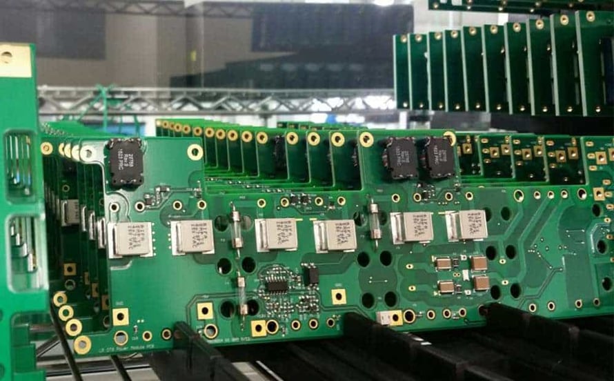
A protector that sits ten millimetres away from the connector does very little, because the trace between them carries the surge current and the inductance of that trace raises the voltage at the pin. The device belongs as close to the connector or the exposed point as the layout allows, with a short, wide connection to the return plane.
Placement also creates a stub. The branch from the signal trace to the protector adds a length of line that reflects and resonates, and its effect grows with data rate. Keeping that branch shorter than a small fraction of the rise time distance is the goal, which in practice means placing the part directly on the trace rather than on a spur, and avoiding long narrow connections to the ground plane.
What The Layout Must Do
The return path of the surge is as important as the signal path. Current that enters the pin through the protector must leave through the ground plane with minimal inductance, which means several vias directly under the device rather than a single thin trace to a distant ground. A protector with an excellent clamp and a poor return path will let the voltage at the pin rise anyway.
Routing the protected pair together and keeping the return reference continuous under them preserves the differential impedance while the protection is present. Where the interface uses guard rings or dedicated protection structures on the board, the protector and the structure should be planned together, so that the current path is defined rather than incidental.
Matching The Part To The Interface
The selection process starts with the interface, not the catalogue. Establish the maximum normal signal voltage including overshoot and common mode, the damage threshold of the receiving device, the required bandwidth, and the surge level the product must survive. Only then compare devices, and compare them on all four axes rather than on clamp alone.
Where the interface is exposed at a connector that a user can touch, the requirement is usually an IEC 61000-4-2 contact discharge level, and the test is performed on the finished product rather than on the component. That puts the emphasis on the board layout and the current path as much as on the silicon, and it means the traces that run to the board edge deserve specific attention during review.
Verification Before Release
Two measurements answer most of the questions. The first is the eye diagram with the protector fitted and with it removed, at the highest data rate the interface supports; the difference is the cost of the protection in signal quality. The second is the clamp voltage measured at the pin under the specified surge, using the final layout rather than a test fixture.
Both measurements are cheap compared with a field return, and both are routinely skipped. A design that passes the eye with margin and clamps below the damage threshold at the connector has done what a TVS diode is for, and the routing of the high frequency nets between connector and receiver is the part of it that determines the outcome.
Checks Before Release
The checks that matter are the ones performed on the product rather than on a sample kept for the purpose, because a coupon that travels with the panel is the only evidence about that panel. Where a requirement can be measured, it should be measured at the point of manufacture and recorded against the board or the lot it applies to.
FAQ
Can a single protector cover several lines? Yes, in an array package, and the array has the advantage of matched capacitance between channels because the devices are made on the same die. The disadvantage is that a fault on one channel can affect the neighbours, and that the package may force a longer stub.
Does a lower capacitance always mean better signal quality? Not by itself. The capacitance matters relative to the impedance and the data rate, and a very low capacitance device with a poor clamp or a long connection to the plane can perform worse overall than a slightly slower part placed correctly.
Is a protector needed on an internal interface? Usually not, unless the board can be handled while powered or the interface is routed to a connector the user can reach. Protection is a response to an exposure path, and identifying that path is the first step of the selection.