Practical Notes on ESD Protection
Electrostatic discharge is a fast, high current event that arrives through the outside world: a cable, a connector, a screw, a finger touching a metal part. The board cannot stop the event from arriving, so the design has to decide where the current goes when it does. Every effective measure does the same thing, which is to give the discharge a short, wide path to chassis ground that does not pass through a signal input on the way.
How ESD Reaches the Board
The current enters through any conductor that connects the board to the outside. A connector on the front panel is the obvious entry point, but a mounting screw bonded to a metal chassis, a metal standoff, or a shield can all carry it in. What matters for the design is that the entry point is known, because protection is placed at that point rather than spread evenly over the board.
The damage is not always catastrophic. A discharge may destroy a device outright, but it is more likely to inject charge into a signal line, where it appears as a transient that the receiving circuit misinterprets, or to shift a node far enough to put the device into a latched state that persists after the event has finished. A board that resets occasionally in the field is often a board with an ESD path that reaches a signal before it reaches ground.
Stack-Up and the Ground Grid
A multilayer board is the starting point, and for a specific reason. A ground plane and a power plane arranged close together reduce the common mode impedance and the inductive coupling between conductors to a fraction of what a two layer board provides, and the improvement is one or two orders of magnitude. Every signal layer should sit next to a plane, so that the return path for a transient is directly beneath the trace carrying it.
Where the design uses a grid of power and ground rather than solid planes, the grid has to be tight to be effective. A spacing of 60 millimetres is the outer limit and 13 millimetres or less is preferable, with connections made wherever the vertical and horizontal runs cross. How the ground conductors are planned is covered in ground routing and power trace planning.
<img src="https://www.gopcba.com/wp-content/uploads/2026/08/pcb3.jpg" alt="ESD protection layout with guard ring on a PCB” />
Connector Placement and Chassis Ground
Connectors are placed on one side of the board where the design allows it, so that the entry points are grouped and the protection can be concentrated there. The power connection is brought in through the middle of the board where possible, away from the areas most exposed to a discharge, and the input and output circuits sit next to their own connectors rather than being routed across the board.
Beneath any connector that faces the outside world, every layer carries a wide chassis ground or a polygonal ground pour, and those pours are connected together with vias at intervals of roughly 13 millimetres. The result is a low impedance path from the connector shell to the chassis ground on all layers, which is the conductor the discharge current is meant to use. Where the board is mounted inside a metal chassis, the mounting holes are bonded to the same chassis ground through large pads on the top and bottom layers, with no solder mask over them so that the connection is metal to metal. The rules for those features are set out in board outline and mounting design.
Guard Rings
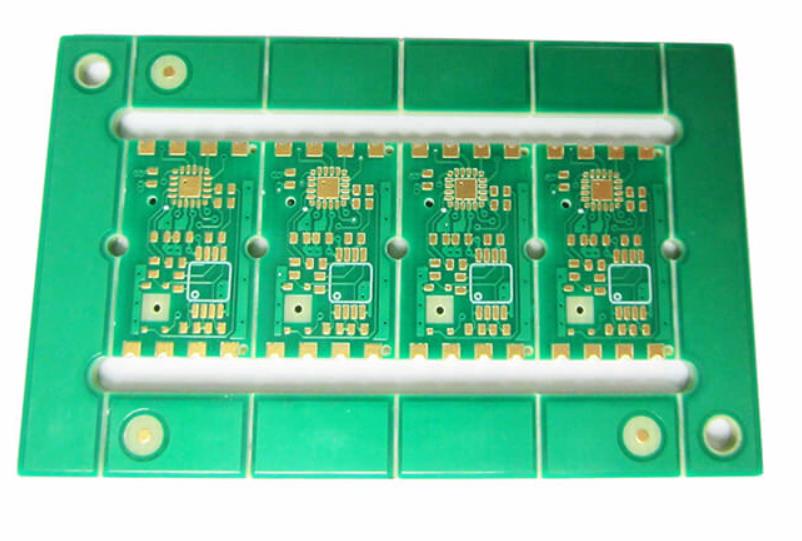
A guard ring is a continuous ground conductor around the perimeter of the circuit, and its dimensions are what make it work. The ring runs around the whole outline except where the edge connector and the chassis ground already occupy that space. It is at least 2.5 millimetres wide on every layer, connected with vias at intervals of about 13 millimetres, and connected to the common circuit ground.
How the ring is terminated depends on the enclosure. On a board that sits inside a metal chassis or shield, the ring connects to the circuit ground. On an unshielded board it connects to chassis ground and is left free of solder mask so that it can act as a discharge point for an arc, and at least one narrow gap, around 0.5 millimetres wide, is left in the ring on every layer so that the ring does not form a large closed loop. Signal traces stay at least 0.5 millimetres away from the ring. The wider topic of how traces near the board edge are handled is covered in ESD and PCB edge traces.
Protection Components at the Connector
Protection is placed at the point where the disturbance enters. A transient suppressor sits at the connector, and the trace from the connector to the suppressor, and from the suppressor to chassis ground, is kept short and wide: less than five times its own width, and preferably less than three times. A long thin connection to a suppressor is a connection that adds inductance, and inductance is what turns a fast discharge into a voltage spike.
Signals enter the board through the suppressor before they reach anything else. A bypass capacitor is placed close to the connector, or within about 25 millimetres of the receiving circuit, and connected to chassis ground or to the receiving circuit ground with the same short, wide geometry. A series resistor or a ferrite bead at the receiver limits the current that reaches the input, and where the connector drives a cable that is itself exposed, a series element at the driver provides protection from that direction as well. Where a converter or a sensor shares the board with digital logic, the same separation discipline applies, and is described in mixed-signal PCB design guidelines.
Loop Area and Signal Routing
The loop formed by a signal and its return is the antenna that couples a transient into the circuit, so keeping the area small is the most general ESD measure available. Where a signal has to travel a long distance across the board, the return path should change sides periodically so that the loop does not accumulate area. Any signal longer than about 300 millimetres should have a ground trace running parallel to it, and where several receivers are driven from one source, the signal should be taken from the centre of the network rather than from one end so that the branches are balanced.
The supply loop matters as much as the signal loop. A high frequency capacitor at every supply pin of every integrated circuit, and a bypass capacitor within about 80 millimetres of every connector, keeps the loop between supply and ground short enough that a transient current does not develop a significant voltage across it. Unused areas of the board are filled with ground where possible, the fills on all layers are joined at intervals of about 60 millimetres, and a large ground fill is connected to ground at both ends rather than at one point. Where an opening in a power or ground plane is longer than about 8 millimetres, a narrow connecting trace is placed across it.
Reset, Interrupt and Control Lines
Reset, interrupt and edge triggered control lines are the signals most likely to cause a visible malfunction, because a transient on one of them changes the state of the system rather than corrupting a single reading. They are routed with high frequency filtering at the input, kept away from the input and output circuits, and kept away from the board edge.
Two further rules apply to the routing around them. A protected signal and an unprotected one are never routed in parallel, because coupling between them defeats the protection. And the board itself belongs inside the enclosure, away from openings and internal seams, so that the discharge has somewhere other than the board to go. Those placement decisions are made at the mechanical design stage, which is another reminder that ESD performance is set by the whole assembly rather than by the board alone.
FAQ
Where should ESD protection be placed? At the point where the discharge enters the board, which in practice means at the connector. Putting it further in lets the transient travel across the board before it is clamped.
Why does the ground connection to a suppressor have to be short and wide? Because the inductance of a long connection turns a fast discharge into a voltage spike. A length under five times the trace width, and ideally under three, is the usual guidance.
How wide should a guard ring be? At least 2.5 millimetres on every layer, stitched with vias every 13 millimetres or so, and separated from signal traces by at least 0.5 millimetres.
Why leave a gap in the guard ring? To stop the ring forming a large closed loop. The gap is narrow, around 0.5 millimetres, and appears at one position on each layer.