Clock Buffer Skew and Fanout Design for Converters
Clock distribution is one of those design tasks that looks trivial until it is measured. A source oscillator drives several loads, a buffer fans the signal out, and the schematic shows a clean tree. On the bench the picture changes: two outputs of the same buffer arrive at slightly different times, the edges are not identical, and a converter sampling on that clock sees an error that the schematic never predicted.
For high-speed converters and serialiser interfaces the relevant quantity is not the buffer’s headline frequency but the difference between its outputs and the stability of the edges over time and temperature. Those parameters are specified separately, and mixing them up is the most common reason a fanout design underperforms. A clock buffer is only useful if the numbers that matter to the load are the ones that were budgeted.
What a Fanout Buffer Has to Guarantee
A fanout buffer takes one input and reproduces it on several outputs, and its job is to do so without adding distortion, delay differences or noise. Each output must swing to the levels the receiving device expects, with rise and fall times short enough for the data rate, and the outputs must be as close to identical as the application requires. Where the input can be disconnected, the buffer also has to define a safe state rather than oscillating.
The last point is a practical one. A differential input left open can float into an indeterminate condition and produce noise that propagates into the clock tree. Buffers designed for this environment include input clamping so that an open input is pulled to a defined level and the outputs are held in a known state, which removes the need for additional external protection circuitry and the layout area it consumes.

Skew And Delay Numbers That Matter
Propagation delay is the time from input transition to output transition, and it sets the phase relationship between the source and the loads. Output skew is the difference in delay between outputs of the same device, and it is the parameter that decides whether parallel loads sample simultaneously. Part-to-part skew is a third quantity, relevant when several buffers are used in one system and their outputs must also align.
Modern differential fanout buffers achieve figures in the region of 265 ps of typical propagation delay with only about 5 ps of output-to-output skew, and measured phase difference between two outputs at 1.2 GHz can stay below 10 ps. For a synchronous sampling application that means the two clock edges arrive close enough that no additional phase calibration is required, and operation up to a toggle frequency of 1.5 GHz covers most high-speed converter and serialiser clock requirements.
Additive Jitter and Phase Noise
An ideal buffer would pass the source clock through unchanged. A real one adds a small amount of random noise to the edge positions, which appears as additive phase noise and as jitter in the time domain. For a converter clock the consequence is a reduction in the effective number of bits at high input frequencies; for a high-speed serialiser it consumes part of the timing budget that the link margin depends on.
The practical approach is to compare the additive noise of the buffer with the noise of the source. If the source already dominates, the buffer choice is not critical and the effort belongs elsewhere. If the buffer is comparable to the source, its contribution has to be included in the jitter budget, and the measurement should be made on the assembled board rather than taken from a datasheet, because supply noise and layout coupling both raise the figure that the bench shows.
Interfacing and Level Considerations
Fanout buffers are often built in technologies that do not swing to the same levels as the receiving logic, and the interface has to be designed rather than assumed. Emitter coupled logic families, for example, require termination to a supply rail rather than a simple pull-up, and their outputs sit at levels that a CMOS input will not accept directly. Where a temperature compensated version of the same device is available, it holds its parameters more consistently over the industrial range, which matters for equipment that must meet the same timing limit in winter and in summer.
Termination placement is part of the design, not a detail added afterwards. A termination resistor placed at the wrong end of a transmission line produces a reflection that shows up as edge distortion, and a differential pair routed with different lengths converts part of the differential signal into a common-mode component that radiates. Treating the clock distribution as a transmission line problem, as described in high frequency trace routing, is what keeps the measured edges close to the simulated ones.
Layout Rules for a Clock Tree
Clock layout rewards discipline more than cleverness. Keep the distance between the buffer outputs and their loads as similar as the skew budget allows, using serpentine routing for length matching where a deliberate delay is required rather than an accident. Reference each pair to a continuous ground plane and avoid layer transitions where possible, because a change of reference introduces impedance discontinuities at exactly the point where edge timing is most sensitive.
Decoupling is the other half. Each supply pin needs a low-inductance path to ground, placed close to the pin with the shortest possible loop, because supply noise modulates the switching threshold and appears directly as skew. Keep the clock tree physically separated from switching regulators and high-current paths, in the spirit of mixed signal design guidelines, and route it away from connectors and board edges where it can couple into cables. A clock that is clean on the bench but not on the product is usually a layout problem, not a component problem.
Process Control and Verification
Reviewing the design before the data is released is far cheaper than correcting it after the panel is in the tank, because every step downstream inherits the decision made at the front end. Where a value sits close to a process limit, the drawing should say so, since the shop can then open the process window rather than working to a nominal figure that carries no tolerance.
The measurements that matter are the repeatable ones: conductor width and spacing, annular ring, finished hole size, plating thickness and surface finish are all verifiable on a coupon that travels with the panel. Documenting the assumption is part of the design work, and a short note on the drawing prevents a question that would otherwise arrive a day later and cost a day of schedule.
Measuring a Clock Tree on the Bench
A clock distribution network should be measured where it matters, which is at the input of the receiving device rather than at the buffer output. Use a probe with sufficient bandwidth, because an oscilloscope front end that is too slow will show a clean edge that does not exist, and measure the pair differentially so that common-mode noise is not mistaken for timing error. Compare the two clock inputs to each other directly when phase alignment is the requirement.
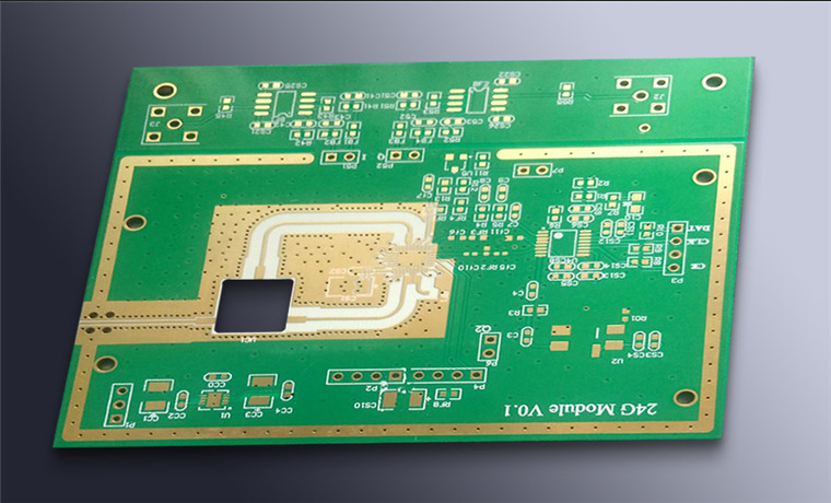
Two measurements are worth recording. The first is the phase difference between the two loads at the highest operating frequency, which is the quantity that decides whether simultaneous sampling works. The second is the edge quality, including overshoot and any step that indicates a reflection, since a distorted edge shifts the effective sampling instant. Record both over temperature if the equipment is specified to operate across a range, and repeat the measurement after any change to termination or routing.
FAQ
Which skew figure should be budgeted? Use output-to-output skew when several loads must sample together, and part-to-part skew when several buffers are used. They are different parameters and only one of them describes the situation in the design.
Does a faster buffer always improve jitter? No. Output edge rate and additive noise are separate characteristics, and a device with very fast edges can couple more noise into the surrounding circuitry. Match the edge rate to the requirement.
Is an enable pin worth having? Yes when the clock must be gated for power saving. A buffer with a defined enable threshold lets a GPIO turn the clock off, removing the need for a separate clock switch and its associated skew.