MI And CAM: What Happens After Gerbers Arrive
Sending a set of gerber files to a fabricator starts a process that most designers never see, and the questions that come back a day later are the visible part of it. Behind those questions sit two engineering functions: the CAM department, which converts the artwork into machine data, and the MI engineer, who writes the manufacturing instruction. Between them, MI and CAM decide how the board will actually be built.
Understanding what those functions do explains most of the questions that arrive during fabrication, and it explains why supplying a complete package at the start is faster than answering queries one at a time.
The work is not clerical. Both functions have to reconcile what the design requires with what the process can hold, and every reconciliation that has to be referred back to the designer costs a day of schedule.
What CAM Does With The Artwork
CAM software reads the gerber layers and converts them into the form the production equipment needs. That means applying the process compensation the shop knows it needs, adding the tooling and the panel frame, generating the drill and routing programs, and creating the solder mask and stencil data from the layers it has been given.
The compensation is the part designers underestimate. Etching removes copper, so the artwork is biased outward to produce the correct finished width. Plating adds copper, so the inner layer artwork is biased smaller. The amount of bias depends on the copper thickness and on the shop’s own process, and it is not something the design can specify.

Panelisation And What It Determines
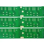
A board is not built alone. It is placed on a production panel with other boards, or with multiple copies of itself, and the arrangement determines how many boards fit on a panel and therefore a large part of the cost. Panel size, spacing between boards, breakaway rail width and the method used to separate them are all decided at this stage.
The separation method matters for the design. V-scoring applies a mechanical cut that leaves a controlled web, and it works on straight edges with sufficient board thickness. Routing with tabs works on any outline but leaves burrs and requires the tabs to be removed afterwards. Where the design has components close to the edge, the clearance needed by the separation method has to be respected in the layout, and the panelisation and breakaway design therefore starts as a layout constraint rather than as a fabrication decision.
What MI Decides
The MI engineer builds the instruction set for the specific board: the stackup construction with the actual prepreg and core part numbers, the drill schedule with tool sizes and hit counts, the plating thickness targets, the surface finish selections, and the inspection plan. Where the design specifies a finished dielectric thickness, the MI engineer selects the combination of materials that will produce it after lamination.
This is where the questions originate. A stackup that names a layer thickness but not a construction can be built in more than one way, and the two ways may differ in impedance. A drill table that mixes hole sizes can be simplified or may need to be kept separate. A via that must be filled and capped needs a process step that has to be scheduled.

Documentation travels in both directions. A shop that returns the panel drawing and the stackup it intends to build is giving the designer a chance to confirm that the interpretation matches the intent before any material is cut. Reviewing that document takes minutes and catches the mismatches that would otherwise appear as a query during production.
The Engineering Query
An engineering query is the mechanism for resolving a discrepancy between the design and the process. It is not a complaint; it is a request to confirm an interpretation, and answering it promptly is the single largest schedule lever available to the designer once the board is in the shop.
Common queries concern a missing solder mask opening, a silkscreen line that is narrower than the process can print, a hole size that is smaller than the minimum for the finished board thickness, and a copper feature that violates the minimum spacing. Each of these can be resolved in minutes with a clear answer, and each can lose a day if left in an inbox.
What The Package Should Contain
A complete release package contains more than the copper layers. It should include the board outline with tolerances, the stackup with materials and thicknesses, the drill file and drill table with plating requirements, the impedance requirements naming the nets and the layers, the surface finish for each area, and the fabrication notes covering panelisation, marking and inspection.
Supplying the layers without the notes forces the shop to make assumptions, and each assumption is a query. The prototype order checklist is a useful way to verify the package before it is sent, because the items it contains are exactly the ones that generate questions when they are missing.
Where Tolerances Come From
The tolerances quoted in a fabrication drawing are not free parameters. They are the sum of the tolerances of the processes the board will pass through: imaging, etching, lamination, drilling, plating and routing. Tightening one of them without tightening the others produces a drawing that cannot be met, and a shop that quotes to the drawing anyway will deliver a board that is nominally compliant and functionally marginal.
Choosing tolerances that match the capability of the intended process is the practical approach, and the manufacturing tolerance figures a shop publishes are the best guide to what it can hold. Where a design genuinely needs a tighter figure, that should be stated for the specific feature rather than applied to the whole layer.
Making The Process Faster
Three habits shorten the interval between sending files and receiving boards. The first is a complete package, so that no queries are needed. The second is a stackup that names materials and constructions rather than only thicknesses, so that MI does not have to choose. The third is a fabricator who has built the same stackup before, because the first time a shop runs a combination it has to characterise it.
None of these is a technical subtlety; they are process decisions. A design that is easy to build is not a design that compromises performance, it is a design whose author understood what the factory needs in order to reproduce the intent.
It also helps to know which changes are free and which are not. Substituting one prepreg part number for another of the same construction is usually invisible. Changing the number of layers, the finish or the panel arrangement after the panel has been released for production is not, and it will usually move the board to the end of the queue.
FAQ
Do gerber files carry the design intent? Partly. Gerber describes geometry, not purpose, so a feature that exists for a specific reason must be explained in the fabrication notes or it will be optimised away. The newer formats carry more structure but still need a notes document.
Can I specify the panel layout myself? You can propose it, and it is often worthwhile when the board has an unusual shape, but the shop has to confirm it against its own handling and tooling constraints.
Why does the same design cost different amounts at different shops? Because the panel utilisation, the process steps required, the yield at the shop’s capability and the number of layers needing controlled impedance all differ. Comparing quotes without those details compares prices rather than offers.