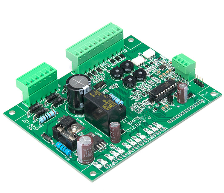
PCB Panelisation: V-Cut, Stamp Holes and Spacing
Very few boards are built one at a time. Several copies, or several different designs, are combined into a panel so that the fabricator and the assembly line handle one object instead of many, and the way they are joined decides both the cost and whether the edges survive the process.
This article covers the two methods of holding a panel together, the spacing that the array requires, and the framing and tooling that the assembly equipment needs in order to place components on it.
Why Boards Are Combined Into Panels
A panel is the working unit for every machine in the process. Drilling, plating, imaging, solder mask, assembly and test are all set up once and then run over the whole panel, so a panel that carries more boards has a lower cost for each of them.
There is also a practical limit. Very small boards cannot be handled or clamped on their own, and assembling them in a panel is the only way to place components on them at production rates. Panelisation is therefore not only an economy: for a small board it is a requirement.
V-Cut Scoring
Scoring cuts a groove along both surfaces of the panel on the same line, leaving a thin web of laminate that holds the boards together and snaps by hand when the panel is broken apart. The groove is produced with a rotating blade, and the depth of the cut on each side is controlled so that the remaining web has enough strength to survive the process and not so much that the board cannot be separated cleanly.
Because the blade runs across the panel, scoring works only along straight lines that extend across the whole panel. The clearance from the score line to the nearest copper, and the direction the board is broken, both belong in the design, and the rules are covered in the notes on slot and edge routing.
Stamp Holes and Breakaway Tabs
Where an outline is curved, or where scoring would cross a feature that must not be cut, the board is held by tabs that break along a line of small holes. The holes are drilled in a row like the perforation of a stamp, and the tab between them breaks when the board is flexed.
This method allows any outline shape and does not damage either surface, which makes it suitable for boards with components close to the edge. The penalty is that the tabs leave small protrusions where they break, and for a board that has to fit a close-tolerance opening those have to be removed by a second operation.
Spacing and the Array Layout
The spacing between adjacent boards in the array is set by the method that joins them. Boards placed exactly one board width apart touch, which is the arrangement that scoring requires, because the score line lies on the shared edge.
Where a gap is used instead, the gap has to be wide enough for the tab and the perforation, and it can never be narrower than the board, because that would mean the boards overlapped. The gap is where the perforated tabs are placed, and its width is chosen so that the router or the punch can cleanly form the edges of both boards.

Frames, Rails and Tooling
A panel normally carries a border, called the frame or the rail, around the array of boards. The rail is what the conveyor grips, what the tooling holes are drilled into, and what the assembly machine clamps when it holds the panel in position.
The width of the rail is set by the equipment that will handle the panel rather than by the boards. Where the assembly line needs a wider edge than the fabricator would choose, the requirement comes from the assembly house, and it is agreed before the panel is laid out rather than discovered when the panel arrives.
Fiducials and Machine Readability
Placement machines find the panel by looking for fiducials: small copper marks with a clear area around them, placed on the panel and on each individual board. Panel fiducials let the machine align to the panel as a whole, and board fiducials let it correct for the small positional differences between one board and the next.
Without them, the machine relies on the mechanical position of the panel in the fixture, and the accumulated tolerance is enough to place a fine-pitch part off its pads. The marks also need contrast, which means no solder mask over the copper and no legend nearby, and their placement follows the rules for outline features.
Panelisation and the Assembly Process
The panel is the unit that goes through the printer, the placement machine and the reflow oven, and its shape affects all three. A long thin panel can sag in the oven, a panel whose boards are arranged unevenly heats unevenly, and a panel that is too large for the conveyor cannot be run at all.
Where component density varies across the panel, the placement order and the paste printing are planned around the panel rather than around one board, which is why the array layout and the assembly process are discussed together. The guidelines that keep a design manufacturable apply to the panel as well as to the board.
Data for the Panel
The panel is a separate design file in most workflows. The board is copied into it, the array is created by pasting further copies at a defined spacing, and the reference designators are incremented so that each board can be identified during assembly and test.
The panel file also carries the rails, the tooling holes, the fiducials and the score or tab details, and it is the file that the fabricator and the assembler both work from. Because it is derived from the board rather than being the board, it has to be regenerated when the design changes, and the checks that precede a prototype build include confirming that the panel and the board agree.
Score Depth, Web Thickness and Break Quality
The web left behind by scoring is a compromise. Too little material and the panel separates during handling or assembly; too much and the board will not break cleanly, leaving a rough edge that has to be trimmed and a risk of delamination along the fold.
The depth is usually specified as a proportion of the board thickness rather than as an absolute dimension, because the two blades approach from opposite faces and the remaining web is what matters. It is also checked against the component keep-out, since the material removed at the surface is exactly the material that the copper clearance was calculated from.
FAQ
Which joining method should be chosen? Scoring where the edges are straight and the components are clear of them, and tabs where the outline is curved or the edge is crowded. Cost and the assembly method usually decide between them.
How much material is wasted on a panel? The rails and the gaps between boards. A well planned array keeps both to the minimum the equipment allows, which is why the rail width is agreed rather than assumed.
Can different designs share one panel? Yes, and it is common where the quantities are small. Each design keeps its own circuit data, and the panel simply carries several of them into the same process cycle.