
HDI Build Cycles and PCB Lead Time
An HDI board is not simply a multilayer board with smaller holes. It is built in cycles, and every additional cycle adds a lamination, a drilling operation and an inspection step that cannot be compressed by working faster. Understanding hdi build cycles is therefore the only honest way to predict PCB lead time, and it is the reason a fourteen-layer three-stage design quotes very differently from a fourteen-layer conventional stackup of the same outline.
Why HDI Is Built in Cycles
In a conventional multilayer board, every layer is imaged and etched before a single lamination joins the whole stack. The vias are then drilled through the finished panel, plated and finished. The process is long at the front end, but it happens once, and the number of lamination presses is one.
HDI inverts that logic. Because laser-drilled microvias can only penetrate a thin dielectric, layers that must be connected by microvias have to be joined first, drilled, plated, and then laminated again with the next pair of layers. Each pass through that loop is a build cycle, and the total number of cycles is what drives the schedule.
Sequential Lamination Step by Step
A single cycle begins with an inner core that already carries its circuitry. Prepreg and copper foil are laid up on both sides, and the stack is pressed. The outer copper is then thinned, the via targets are imaged, and the microvias are drilled by laser from the newly exposed surface down to the layer beneath. Plating, filling and planarisation follow.
Only after that sequence is complete can the panel become the core of the next cycle. Sequential lamination therefore multiplies not by the number of layers but by the number of times the panel must re-enter the press, and each re-entry carries its own registration risk, its own yield loss and its own queue in front of the equipment.
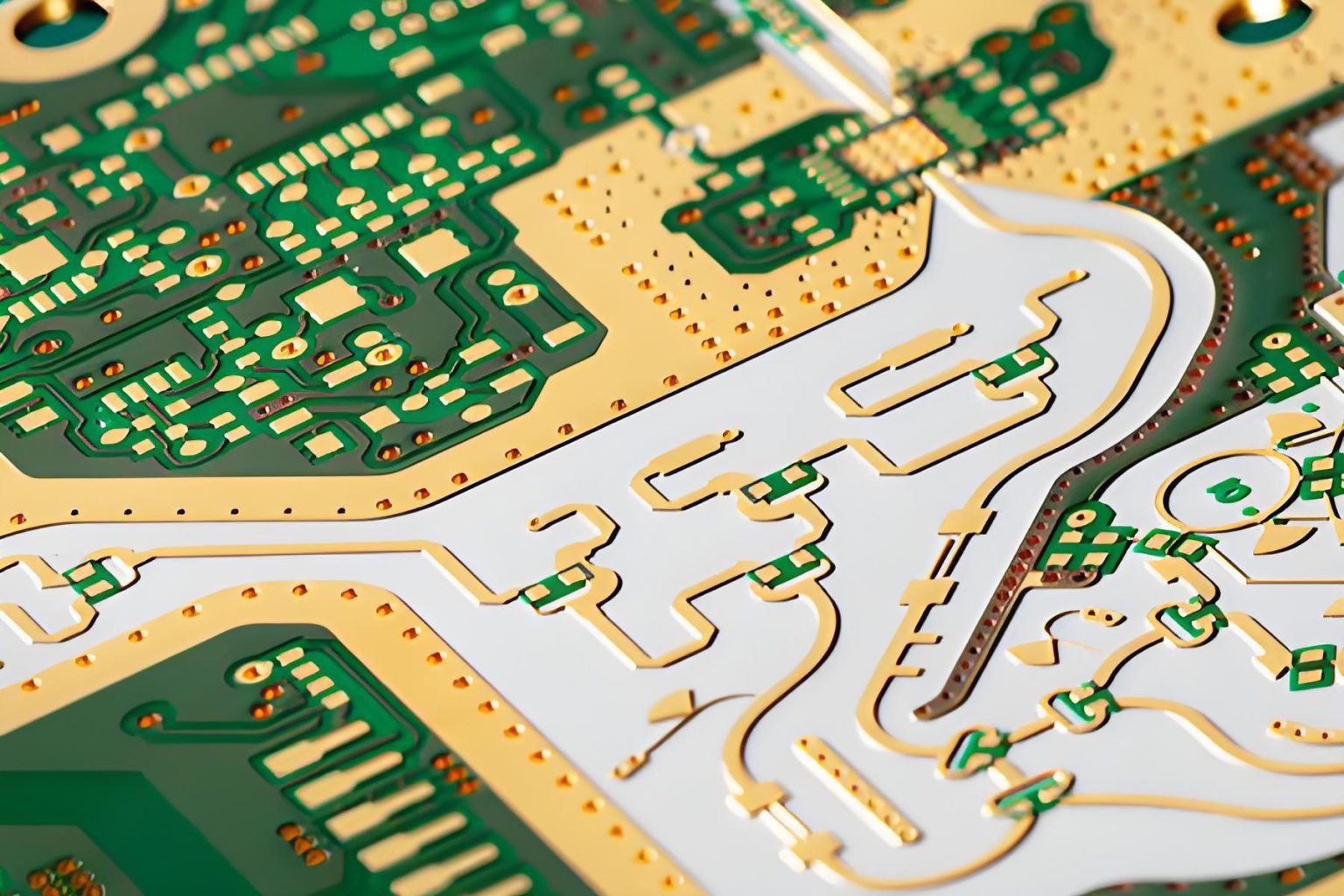
Laser Via Formation and Inspection
Laser via formation is fast, but it is not unconditional. The dielectric has to be thin and uniform enough for the beam to reach the target pad without damaging the layer below, and the copper surface has to be treated so that the laser couples into the dielectric rather than reflecting off it. Window size, energy and pulse shape are all recipe parameters that have to be settled per stackup.
Inspection follows every cycle. Microvias are checked for depth, for wall coverage after plating and for voids in the fill, and the checks are done while the panel can still be reworked or scrapped cheaply. A defect found three cycles later costs the entire build rather than one layer pair, which is why HDI inspection is scheduled inside the cycle rather than at the end.
Layer Count and Stage Count
Two numbers describe an HDI stackup, and they are often confused. The first is the total layer count, which sets the routing capacity. The second is the number of build stages, which sets the manufacturing effort. A 3+N+3 description, for example, means three microvia stages on each side of an N-layer core, not three layers in total.
Stage count grows faster than layer count in cost and time. Adding a stage adds a full lamination and laser cycle to both sides, whereas adding a core layer adds material and drilling without adding a press pass. Our notes on layer stackup from one to eight layers describe how the same reasoning scales from simple boards upward.
Where the Time Actually Goes
Lead time in HDI is dominated by queueing, not by the duration of any single operation. Laser drilling a panel takes minutes; waiting for the laser, the press and the plating line between cycles takes days. A three-stage board passes the laser and press areas three times, so it inherits three sets of queues.
Material availability is the other hidden term. Thin prepreg, low-profile copper and the specific dielectric required by a high-speed stackup are stocked in fewer widths and thicknesses than standard FR-4, so a build can wait on a material that is not in the plant. Our notes on HDI lamination structure explain how the layer construction itself constrains those choices.

Planning the Schedule Around Build Cycles
Because the cycles are serial, the only real lever on lead time is the number of cycles. Reviewing the stackup with the fabricator before the design is frozen will often show that the same routing capacity can be reached with two stages instead of three, or with a thicker core and one fewer lamination pass, at no cost to the electrical performance.
Early release of the stackup also helps. Engineering questions about dielectric thickness, via fill and registration tolerances are answered while the design is still open, so the panel does not sit in a hold queue waiting for a reply. A day spent on the front end frequently saves a week at the back end.
Design Choices That Shorten Lead Time
Designing for the process is not the same as lowering the specification. Keeping microvia stacks simple, avoiding unnecessary stacked vias and using through vias where the routing allows all reduce the number of laser operations per panel and the number of inspection points that can reject it.
Via fill choices matter as much. Our notes on blind and buried via stack selection describe how to match the via structure to the layer it must reach, which avoids the common case of a design that needs an extra stage purely to accommodate one awkward connection.
Asking the Right Questions Before Ordering
When an HDI quotation arrives, the useful questions are about the build rather than the price. How many lamination cycles does this stackup require, which operations are sequential, and which of them is the schedule constraint in the plant at the moment the order is placed? The answers explain most of the variation between quotes.
At gopcb, the stackup is reviewed against the intended build cycles before quoting, so that stage count, via structure and material are agreed before the panel enters the queue. The result is a lead time that reflects the real process rather than an optimistic estimate made at the quotation desk.
Stackup Choices That Add a Cycle
The most expensive mistake in HDI planning is asking for a connection that no single cycle can make. If a signal must travel from the outer layer to a plane four layers down, and the design also requires that the intervening layers be laminated separately for other reasons, the process has to add a stage to reach it. Redrawing that one net can remove an entire press pass from the build.
A second common cause is an unnecessarily thin dielectric. Thin prepreg is what makes laser drilling possible, but it is also harder to laminate uniformly, so a stackup that uses the thinnest available material for every layer will attract more rework and more inspection holds than one that uses thin material only where a microvia actually needs it. Thickness should follow function, not habit.
The third is registration margin. Each lamination cycle adds a new opportunity for layer-to-layer misalignment, so a design that places microvia targets close to the edge of their capture pads, or that leaves no room for the normal registration tolerance of the press, will generate engineering queries and possibly a rebuild. Generous capture pads cost a little routing space and buy a great deal of schedule.
FAQ
Does more layers always mean a longer lead time? Not by itself. A conventional fourteen-layer board with one lamination can be faster than a six-layer HDI board with three build stages, because the cycles, not the layer count, dominate the schedule.
Can build cycles be reduced after the design is finished? Sometimes, by combining stages or converting a microvia connection to a through via, but the change usually touches routing. Reviewing the stackup early is far cheaper than revising it later.
Why do two quotes for the same stackup differ so much? Usually because one assumes a simpler build or different material. Comparing the number of cycles and the specified prepreg is more informative than comparing the total price.