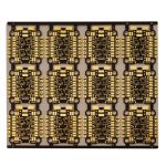
HDI Lamination and Structure: Sequential Build-Up with Resin Coated Copper
High density interconnect boards are not made by drilling smaller holes in a conventional stack. They are built in stages, adding a pair of thin, dense layers on top of a finished core, then repeating the cycle if the design demands it. HDI lamination and structure therefore describe a manufacturing sequence as much as a stackup, and the material choices at each stage determine how fine the resulting vias and traces can be.
What Sequential Build-Up Actually Means
Sequential build-up, usually abbreviated SBU, adds dielectric and copper layers one pair at a time. After each addition, the new layer is laser drilled, plated, imaged and etched before the next one goes on. This differs fundamentally from conventional multilayer processing, where every layer is fabricated flat and then bonded together in a single press cycle.
The advantage is that fine features are produced on a thin, already-supported surface rather than on a free-standing core, which is what makes very small vias practical. SBU also supports solid filled vias, which improve thermal management, strengthen the interconnection between layers and raise overall board reliability compared with stacked or unfilled structures.
The Core plus Build-Up Architecture
The most widely used HDI structure takes a conventional printed circuit as its starting point. That core may be single sided, double sided, multilayer, or already contain buried and blind vias. Two to four higher density layers are then built onto one or both faces, producing what is often called a core plus sequential laminating structure.
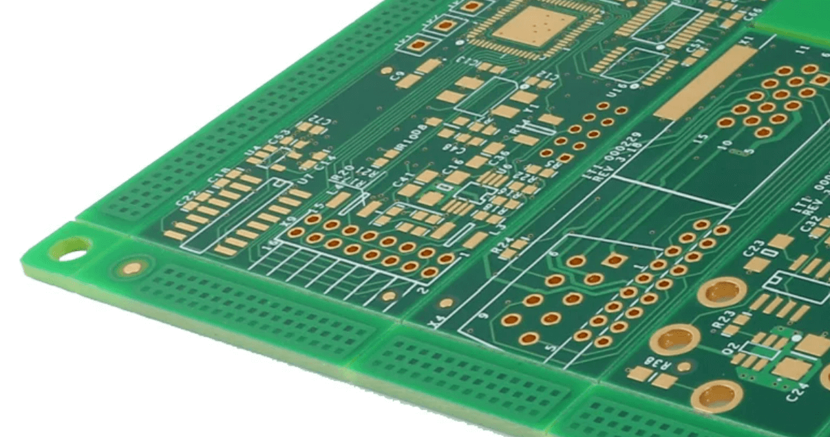
Because the core itself can be almost any conventional construction, the family of possible structures is large. The appeal of this architecture is leverage: existing fabrication equipment produces the core, and only the build-up steps require HDI capability. The rigid core supplies the mechanical skeleton and the flatness, while the thin added layers deliver the routing density.
Resin Coated Copper as a Build-Up Material
Build-up layers are usually formed from resin coated copper, a material developed specifically for this role. It combines an extremely thin copper foil with a resin layer bonded to it, and the foil surface carries microscopic nodules to provide adhesion. The whole sheet is chemically treated and primed so that it can hold the finest lines and spaces the process can print.
The material is not without cost. Resin coated copper is known for poorer hole quality and longer drilling times in mechanical operations, and it behaves differently from conventional prepreg during laser processing. In exchange, it permits a much thinner overall construction, which is exactly what a high density design needs in order to keep the finished board within its thickness budget.
Laser Via Formation and Dielectric Control
Vias in the build-up layers are formed by laser, most commonly a carbon dioxide source operating in the 9.4 to 10.6 micrometre band. Finished microvia diameters typically fall between 100 and 200 micrometres. Achieving that consistently depends less on the laser than on the dielectric above and below it, since the pulse must open the resin cleanly and stop at the underlying copper.
Resin thickness in the coated copper is therefore tightly specified, generally between 40 and 80 micrometres, to keep the dielectric layer thin and uniform. Some constructions use a partially cured resin, roughly half cured with the remainder still in a B-stage condition, so that the material flows into trace gaps during lamination while still bonding the layers and holding the target dielectric thickness.
Laminating Dry Resist onto HDI Cores
Dry resist is still applied to build-up laminates using heated rollers, which is an older technique. Modern practice preheats the material to a set temperature before lamination rather than relying on the rollers alone. Preheating lets the resist stabilise against the laminate surface, draws less heat out of the rolls, and produces a consistent exit temperature across the panel.
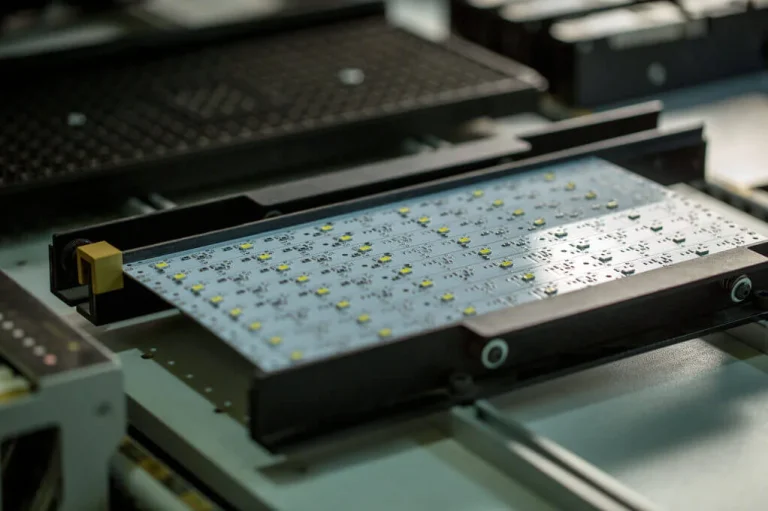
Consistent entry and exit temperatures matter for a specific reason: they reduce the air trapped beneath the film. On coarse geometries that air is a cosmetic nuisance, but on HDI layers it directly degrades the reproduction of fine lines and spacing. Where the resist does not wet the surface evenly, the imaging step will not resolve the features the design requires.
Where HDI Lamination Goes Wrong
Build-up defects cluster around a few causes. Resin that is too thick prevents reliable laser via formation. Resin that flows too far leaves thin dielectric over traces. Insufficient flow leaves voids that appear later as delamination or as plating defects inside a via. Because the layers are thin, there is very little margin in any of these directions.
Panel handling is the other common source. Build-up layers are fragile before they are fully cured, and mechanical damage at this stage is difficult to detect and impossible to repair. Registration between the core and the new layers must also be verified at every build-up stage, since errors compound rather than cancel.
Design Consequences of the Build-Up Structure
The structure dictates some design rules directly. Microvias should be placed over copper rather than in open areas, via stacks need to be evaluated for reliability, and the number of sequential build-up cycles should be kept to the minimum that meets the routing requirement, because each cycle adds cost and risk. Dielectric thickness and via diameter have to be considered together, not separately.
It also helps to decide early how much of the design belongs in the core. Moving dense routing into the build-up layers relieves pressure on the core, but concentrating everything there can force an extra build-up cycle. At gopcb we review HDI stackups alongside the fabrication route so that the layer count and the build-up sequence are chosen together. Related material appears in HDI board CAM methods, blind and buried via stack selection and HDI PCB prototyping.
Verifying Each Build-Up Layer Before the Next One
Because build-up stages are sequential, a defect that is not caught early gets buried under the next layer permanently. Inspection between stages therefore carries more weight than final inspection does. The critical items are laser via cleanliness, plating fill quality inside the microvia, registration against the core, and the actual dielectric thickness achieved over traces rather than over open laminate.
Cross-section coupons are the only reliable way to confirm the dielectric profile over copper features, since measurement over flat areas flatters the result. Daisy chain structures on the same panel allow each build-up layer to be electrically tested before proceeding. Where the product will see thermal cycling, interconnect stress testing or highly accelerated stress testing on a dedicated coupon is worth the cost, because microvia reliability is decided by these thin layers rather than by the core.
FAQ
How many build-up layers can be added? Two to four additional layers, applied to one or both sides of a core, cover most production HDI boards. More sequential cycles are possible but each one raises cost and risk, so designs usually minimise them.
Why is resin coated copper used instead of prepreg? It allows a much thinner dielectric with tightly controlled thickness, which is what makes small laser vias reliable. Prepreg alone cannot hold that tolerance in such a thin layer.
What laser forms the microvias? A carbon dioxide laser in the 9.4 to 10.6 micrometre band is the common choice, producing vias of roughly 100 to 200 micrometres. The dielectric stack, not the laser alone, controls via quality.