Amplifier PCB Design: Gain, Noise and Thermal Control
An amplifier pcb is built around a simple task, which is to make a small signal larger without changing it in any other way. Everything difficult about the design follows from the second half of that sentence. Gain is easy to obtain; gain without added noise, distortion, oscillation or thermal drift is what the layout has to deliver, and the layout is where most designs succeed or fail.
What an Amplifier PCB Does
The board carries the active devices, the passive network that sets the gain, the supply decoupling and the input and output interfaces. Its job is to keep the signal path short and predictable while the surrounding supply and load currents are doing something quite different and much larger.
Amplifier boards appear in audio equipment, instrumentation, communications links, sensor front ends and motor drives. The circuits differ, but the constraints are shared: the input is fragile, the output is powerful, and the two must not be allowed to meet anywhere except through the amplifier itself.
Core Components and Placement
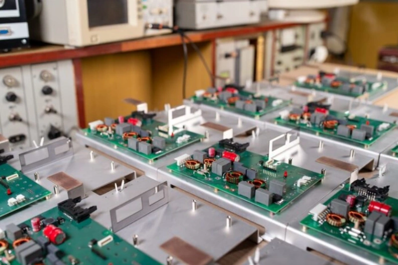
Operational amplifiers or discrete transistors provide the gain, resistors and capacitors set the operating point and the frequency response, and inductors appear in radio frequency stages where resonant tuning is required. Power devices add a heatsink or a thermal pad, and connectors define where the signal enters and leaves.
Placement follows the signal path. Input devices sit close to the input connector, gain stages follow in order, and the output stage sits near the load. Sensitive analogue parts are placed away from the supply entry point, a principle that applies equally to a small audio board and to a mixed-signal instrument.
Setting Gain Without Losing Stability
Signal gain is set by the feedback network, and the feedback path has to be short. A long trace between the output and the inverting input adds capacitance and inductance that change the loop response, and at best that reduces bandwidth while at worst it produces an oscillation that only appears with a particular load.
Compensation components should sit directly against the device pins they serve. Where a stage is expected to drive a capacitive load, an isolation resistor or a small output network is placed at the device rather than at the connector, so the correction acts where the problem is created.

Protecting the Noise Floor
The noise floor is set by the first stage and by everything that couples into it. A ground plane underneath the input network shields it from the rest of the board, and keeping the input loop small prevents it from acting as an antenna for whatever the output stage is radiating.
Component choice contributes as much as layout. Metal film resistors in the input network add less noise than carbon types, and capacitors in the signal path should be selected for the frequency band rather than for price. The layout cannot recover noise that the components themselves generate.
Thermal Management for Power Stages
Power amplifiers convert a large fraction of the supply into heat, and the board is part of the thermal path. A copper area under the device, connected to the package pad by an array of thermal vias, spreads that heat across the plane and into the enclosure.
Sizing the copper is a calculation rather than a guess. Device dissipation, ambient temperature, airflow and the thermal resistance of the assembly determine how much area is required, and the power trace planning that carries the load current is drawn at the same time so the two requirements do not conflict.
Supply Decoupling and Ground Strategy
Every stage needs local decoupling, placed at the device rather than at the edge of the functional block. A small capacitor handles the high frequency current demand and a larger one covers the slower variation; the trace between the two and the device pins should be as short as the layout allows.
The return path matters as much as the supply. A continuous ground plane under the amplifier gives every signal a reference immediately beside it, and where the plane must be divided, the split belongs between functional blocks rather than beneath a single stage. General converter layout rules apply directly to the switching supply that often feeds the amplifier.
Audio, RF and Instrumentation Differences
Audio designs care about distortion and about current delivery into a loudspeaker, so output copper is wide and the supply is heavily decoupled. Radio frequency designs care about impedance, so traces become transmission lines and every millimetre of unmatched path costs return loss.
Instrumentation amplifiers sit between the two. They need very low noise at low frequency, high common mode rejection and often guarded input routing, which puts a premium on symmetry and on keeping leakage currents away from the input nodes.
Verification Before Release
Simulation is worth the effort on an analogue board because the failure modes are subtle. Loop gain, phase margin, noise contribution and thermal rise can all be estimated before the first prototype, and each of those checks is far cheaper than a re-spin.
The prototype then confirms what simulation cannot: real component tolerances, parasitic effects, thermal behaviour in the enclosure and the behaviour of the actual load. Measuring the noise floor and the frequency response of the first board gives the numbers needed to decide whether a second iteration is justified.
From Prototype to Production
Amplifier boards change little between the first article and volume, which is an advantage. The stackup, the layout and the thermal solution are fixed early, and the work that remains is qualifying the supplier, confirming test coverage and making sure the bill of materials is available in the quantities required.
One production issue deserves early attention: the copper weight. High current output stages often need heavier copper than the prototype used, and that changes the minimum trace and space the fabricator can hold, so the current calculation should be settled before the design is released.
Material and Stackup Choices
Most analogue amplifier boards are perfectly well served by standard FR-4. The dielectric properties are stable enough at audio and low radio frequencies, and the mechanical behaviour is well understood, which keeps both the cost and the risk low.
Where the frequency rises, or where loss and dielectric absorption begin to affect the measurement, a low loss laminate becomes worth considering. The decision should follow the band of operation and the accuracy required, rather than a general preference for expensive material.
Layout Review Before Fabrication
A short review before the files leave the desk catches most avoidable problems. Check the current-carrying traces against the load, confirm that every decoupling capacitor sits against its device, and trace the return path of the output current back to the supply to make sure it does not pass under the input network.
Then check the assembly detail: thermal pad connections, the polarity of electrolytic capacitors, the access available for measurement probes and the clearance around parts that will run warm. These are simple items, and they are the ones that most often force a second iteration of an otherwise sound design.
FAQ
Why does my amplifier oscillate only with some loads? Because the feedback loop has lost phase margin at a frequency where the load adds capacitance or inductance. Shortening the feedback path and adding isolation at the output device usually resolves it.
How wide should the output traces be? Wide enough to carry the peak load current with an acceptable temperature rise at the copper weight in use. That is a calculation, not a fixed rule, and it changes with layer and thickness.
Does a ground plane always improve an amplifier? Usually, because it establishes a controlled reference and shields the input. It helps least when the plane is fragmented by unrelated digital routing sharing the same area.