Single Sided PCB vs Double Sided PCB for Prototypes
The difference between a single sided and a double sided board is not just one more layer of copper. It changes how the circuit is grounded, how the board is assembled, how much it costs and how quickly it can be turned around. Most prototypes end up double sided, but there are still cases where a single sided board is the faster and cheaper answer.
What Each Construction Is
A single sided pcb carries copper on one face only. Components are placed on the top, connections run on the bottom, and any crossing that cannot be resolved has to be handled with a wire link or by rerouting. The base is usually a thin laminate with a simple mask and legend.
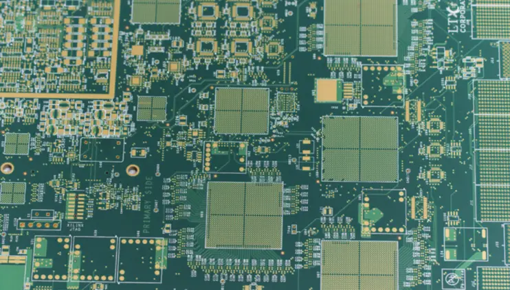
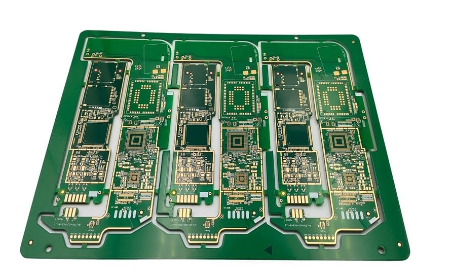
A double sided pcb carries copper on both faces and connects them with plated through holes. That single addition removes the crossing problem, allows a ground plane on one side while signals run on the other, and makes the board compatible with standard assembly processes.
When Single Sided Is Enough
Simple consumer products, power supplies without control logic, LED strips, adapters and low part count circuits are all comfortable on one layer. The rule of thumb is that if the routing fits without more than a couple of jumper links, the second layer is not buying much.
Cost is the reason to stay single sided where possible. The material is cheaper, the process has fewer steps, and the board can be produced in volumes where the saving per unit matters more than the convenience of unrestricted routing.
Why Most Prototypes Are Double Sided
Once a microcontroller, a regulator and a handful of peripheral circuits appear, the crossing count rises and routing on one layer becomes an exercise in compromise. The second layer removes that constraint and usually shortens the design time by more than the board costs.
The ground plane is the other argument. A continuous return path on the opposite face improves noise performance, makes the layout predictable and removes an entire class of problems that a single sided board simply has to live with, as described in general board practice.
<img src="https://www.gopcba.com/wp-content/uploads/2026/08/3.png" alt="Double sided plated through hole prototype PCB with ground plane” />
Routing and Grounding Differences
On a single sided board the ground path is a set of traces rather than a plane, so the return current shares copper with everything else. That is tolerable in a slow circuit and problematic as soon as switching edges get fast or currents get large.
On a double sided board the return path can be made wide and continuous, and vias tie the two faces together where the layout requires. Via placement and sizing follow the usual design rules, including the via annulus and clearance requirements that keep the connection manufacturable.
How Fabrication Differs
Single sided processing skips the plating line, the second imaging step and the second etch. That reduces both cost and cycle time, and it is why a simple board can be turned around in a couple of days while a plated board takes longer.
Double sided processing adds drilling, plating and the second layer of imaging and etching. The solder mask and legend steps are similar on both, though the mask has to clear the plated holes correctly on a double sided board.
Cost and Lead Time
The price difference is modest at prototype quantity and grows with volume, because the material and process savings scale. Lead time follows the process count, so a single sided prototype can often be delivered several days before an equivalent plated board.
Those advantages disappear if the design needs jumper wires, because each link is an assembly step and a potential failure point. A board that is cheap to fabricate but expensive to assemble is not actually cheap.
Assembly Considerations
Single sided boards can be reflowed or wave soldered on one face, and hand assembly is straightforward because everything is accessible. Double sided boards with parts on both faces require two passes or a selective process, which adds tooling and handling.
The mechanical side matters too. Heavier components on a single sided board load the solder joints directly, so mechanical support and the mounting design should be considered at the same time as the circuit rather than after the prototype is built.
Keeping a Prototype Cheap
Use the design rules that the fabricator supports comfortably rather than the tightest ones available. Minimum trace and space that are close to the process limit increase the chance of an etch defect and slow the quotation, while a relaxed geometry costs nothing in performance on a prototype.
Panelise sensibly, keep the outline simple and avoid unnecessary special processes on the first article. Features such as controlled impedance, blind vias or heavy copper can be added once the circuit is proven, when the cost is justified by a working design.
Checking the First Article
Inspect the copper for opens and shorts before assembly, verify that the mask openings match the pads and confirm the hole sizes against the components that will be fitted. These checks take minutes and catch the majority of first time errors.
Once assembled, the prototype should be tested at the extremes rather than at nominal conditions. Supply variation, temperature and load changes reveal whether the grounding and decoupling decisions were adequate, and that information decides whether the board needs another revision before production.
Base Material and Thickness
Most single sided prototypes use a standard paper or glass based laminate, chosen for price and availability rather than for electrical performance. Double sided boards normally use a woven glass epoxy, because the material has to survive drilling and plating as well as soldering.
Thickness is set by the mechanical requirement. A thin board saves weight and cost in high volume, while a thicker one resists bending under a connector or a large capacitor, and the choice affects how the board behaves when a cable is plugged and unplugged repeatedly.
Panelisation and Breakaway
Small boards are produced on a shared panel with tabs or a routed outline, and the way they are separated affects the yield of the finished article. V-score suits straight edges and rectangular shapes, while routed tabs with perforations handle irregular outlines and boards with components close to the edge.
Both methods need space on the panel: a rail for handling, tooling holes for the assembly fixture and clearance around the routing path. Leaving that space in the layout is far easier than discovering at assembly that the fixture cannot hold the board.
Choice of Quantity and Iteration
Prototype orders are usually small, and the temptation is to order the minimum. Ordering a few extra boards costs very little at that stage and often saves a second order when a modification is needed during bring-up, which is common on a first article.
A second iteration should follow the same rules as the first. Changing the stackup, the finish and the outline at the same time as the circuit makes it impossible to tell which change fixed the problem, so revisions are best kept to one category at a time.
FAQ
Can a single sided board have a ground plane? Only a partial one, since the copper on the component side is interrupted by pads and parts. Return paths are formed by traces, which limits how well the design behaves with fast switching.
Is double sided always better? For anything with a microcontroller or a switching supply, usually yes. For a two transistor circuit or a simple LED board, the second layer adds cost without adding capability.
How long does a prototype take? A single sided board can often be turned around in a few days, while a plated double sided board typically needs longer because of the drilling and plating steps.