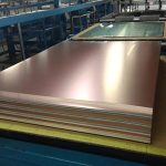
Aluminium Nitride Substrate: Key Checks Before Release
When a power stage has to move a large amount of heat through a thin, electrically insulating layer, the material that does the job is usually a ceramic. Aluminium oxide has served that role for decades, but as switching devices based on silicon carbide and gallium nitride push power density upwards, the thermal resistance of the insulating layer becomes the largest single term in the thermal path. Aluminium nitride is the material that answers that constraint.
An aluminium nitride substrate is not simply a better insulator with a higher conductivity. It changes the design of the whole module: the copper thickness can be reduced, the heatsink can be smaller, and the junction temperature can be held lower for the same load. It also brings process requirements that have to be respected from the powder stage onwards, so treating it as a drop in replacement for alumina usually leads to disappointment.
Why Thermal Conductivity Becomes the Limit
A power semiconductor sits on a die attach layer, which sits on a copper pad, which sits on an insulating ceramic, which sits on a baseplate or a cold plate. Each layer contributes a thermal resistance proportional to its thickness and inversely proportional to its conductivity. Because the ceramic is the only layer that must also be electrically insulating, its conductivity cannot be improved by using metal, and it therefore sets the floor for the whole stack.
Aluminium oxide conducts heat at roughly 24 to 30 watts per metre kelvin. Aluminium nitride conducts at 170 to 230 watts per metre kelvin, which is close to a factor of seven better. In a module dissipating a few hundred watts through a substrate a few tenths of a millimetre thick, that difference is the difference between a junction temperature that is comfortable and one that forces the designer to derate the device.
Properties That Matter Beyond Conductivity
Breakdown strength is high, typically above 15 kilovolts per millimetre, which allows a thin substrate to hold off the working voltage of a traction inverter or a photovoltaic string. Volume resistivity is in the range of ten to the fourteenth ohm centimetres or better. Together these properties let the substrate provide electrical insulation and mechanical support at the same time, removing one interface from the thermal path. That principle is developed further in the notes on thermal management design for power assemblies.
The coefficient of thermal expansion is about 4.5 parts per million per degree, close to that of silicon and silicon carbide. A close match reduces the shear that the die attach and the baseplate joint experience during a temperature swing, which extends the cycle life of the module. Flexural strength is lower than that of alumina, in the range of 300 to 450 megapascals, so the mechanical design has to avoid point loads and sharp edges, and the material must never be treated as a structural member carrying bending stress.
Metallisation and Bonding
Direct bonded copper is the dominant copper metallisation technology. A copper foil is placed against the ceramic and the assembly is heated in a controlled atmosphere until a copper oxygen eutectic forms at the interface and bonds the two together. The result is a strong bond with excellent current capacity, and the copper can be etched into a circuit pattern afterwards. Thick copper is desirable for current capacity but introduces residual stress as it cools, so the pattern geometry has an influence on the flatness of the finished plate.
Active metal brazing uses a titanium bearing braze alloy to wet the ceramic and join it to copper or to another metal. The joint is thinner than a direct bond and the process tolerates nitride surfaces that are difficult to bond directly. Thick film metallisation, in which a metal paste is printed and fired, is cheaper and suits signal and sensor circuits, but it cannot carry the current of a bonded copper layer.
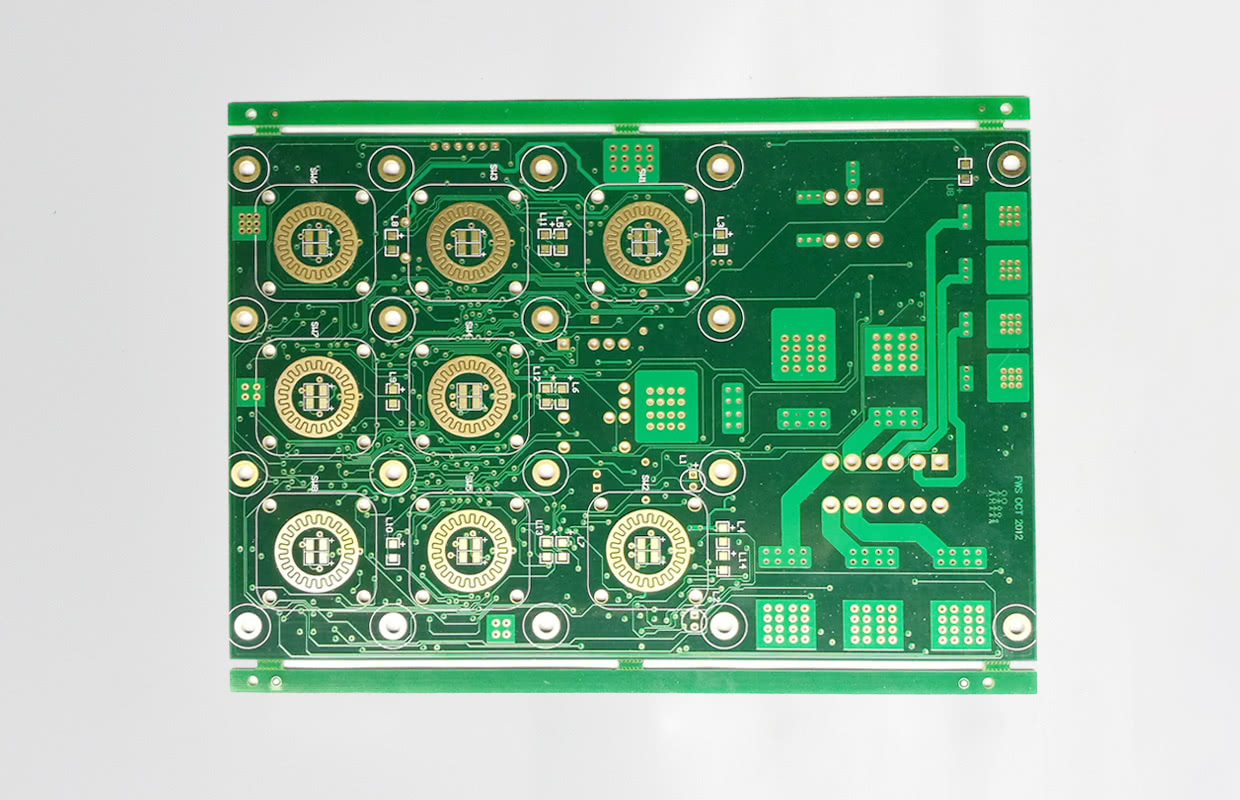
Layout of a Power Module on AlN
The copper pattern on a high power substrate is not only a circuit, it is also a thermal spreader. Wide, short copper areas under each die reduce thermal spreading resistance, and the distance between a die and the edge of the substrate should be kept large enough that heat does not have to travel sideways through a narrow bridge. Thermal vias are not used here in the way they are used on an organic board, because the ceramic already conducts heat directly to the opposite face.
Parasitic inductance in the commutation loop is the other constraint. Placing the high side and low side devices close together and routing the direct current link with a return path directly beneath reduces the loop area and therefore the overshoot at turn off. A well laid out substrate therefore lowers the voltage stress on the devices as well as their temperature, which is why layout and thermal design cannot be separated in a module of this type. Related practice for dense power stages appears in the notes on dc to dc converter layout.
Manufacturing Route and Tolerances
Substrates are formed by tape casting, dry pressing or injection moulding. Tape casting dominates for electronic substrates because it produces large, thin, flat sheets with uniform thickness and reproducible shrinkage. The green sheet is metallised, laminated in the case of a multilayer ceramic, cut to size and then sintered at high temperature. Sintering controls the final density, the grain structure and therefore the thermal conductivity, and oxygen contamination during the process is the main reason a nominally aluminium nitride part measures far below its datasheet value.
Tolerances after sintering are wider than designers expect from an organic board, and they behave quite differently from the manufacturing tolerances quoted for a laminated panel. Thickness may vary by several percent, and the laser or abrasive machining used to singulate the panel leaves an edge that is not perfectly square. The layout should therefore keep metallisation away from the edge and allow for a larger placement tolerance, and the mechanical interface should accommodate the thickness range with a compliant material.
Testing and Reliability
The first measurement is thermal conductivity on a sample from the production batch, because it is the property most sensitive to process drift. Insulation resistance and breakdown voltage follow. For the assembled module, power cycling is the decisive test, since it reproduces the thermal gradient across the substrate that a chamber test does not. The alternating current resistance of the module is monitored during cycling so that joint degradation is detected before it becomes an open circuit.
Where the module will be exposed to humidity, high temperature reverse bias testing is added to check for electrochemical migration and for degradation of the passivation at the copper edges. A cross section after each test confirms whether the failure occurred in the ceramic, at the bond interface or in the die attach, and that distinction determines whether the corrective action belongs with the substrate supplier or with the module assembler, and it is the kind of record that a quality control system has to retain for the life of the product. Any change of powder source or sintering profile should invalidate the previous thermal data and require a repeat of the measurements.
Additional Considerations for This Build
Practical attention to copper metallisation pays for itself here, because it decides whether the finished board behaves as the drawing intended. Where the requirement is not stated on the fabrication drawing or in the assembly notes, the shop has to assume a default, and that default is rarely the value the design was simulated with. Stating copper metallisation explicitly, together with the tolerance that applies, removes the assumption and keeps the result predictable from batch to batch.
Deliberate attention to electrical insulation pays for itself here, because it decides whether the finished board behaves as the drawing intended. Where the requirement is not stated on the fabrication drawing or in the assembly notes, the shop has to assume a default, and that default is rarely the value the design was simulated with. Stating electrical insulation explicitly, together with the tolerance that applies, removes the assumption and keeps the result predictable from batch to batch.
Related reading: our fabrication notes, board quality and design release notes cover the same ground.
FAQ
Is aluminium nitride always better than alumina? No. Alumina is cheaper and mechanically stronger, and where the thermal resistance of the ceramic is not the limiting term, moving to nitride buys nothing. The decision should follow the thermal calculation.
Why does a measured substrate fall short of its rated conductivity? Usually oxygen contamination in the powder or during sintering, and sometimes porosity. Both reduce the phonon mean free path, and the effect is large enough to halve the effective value.
How thick should the substrate be? Thin enough that its thermal resistance is small compared with the device and the heatsink, and thick enough to hold off the working voltage with margin. Below about 0.32 mm the handling and thermal cycling behaviour around bonded copper starts to degrade.