Skills For High Speed Design: Seven Areas That Matter
High speed design is often described as a set of rules to memorise, which makes it sound harder than it is. The rules exist because the interconnect behaves as a transmission line, and once that idea is understood the rules become consequences rather than arbitrary requirements. What a designer needs is a working knowledge of a handful of areas, and the judgement to know which of them applies to the board in front of them.
This article covers those areas in the order that they tend to affect a design, from the power delivery network through the geometry of the routing to the verification that closes the loop.
Each area is worth understanding at the level where the cause is clear, because that is what allows a rule to be adapted when a board does not match the example it came from.
Power Delivery And The Bypass Capacitor
Digital devices draw current in bursts, and the supply has to deliver that current without letting the voltage move far enough to disturb the logic. If the path from the regulator to the device is long and inductive, the surge current turns into high frequency noise that couples into other nets, and the voltage drop across the inductance can be large enough to affect operation.
The bypass capacitor is the local source of charge that keeps the loop small. Its job is not to store energy for the whole board but to supply the device for the duration of an edge, and its effectiveness depends on the inductance of the connection between the capacitor and the device rather than on its capacitance alone. That is why a pair of capacitors, one large and one small, is used to cover a wide frequency range, and why the placement of the via that connects them to the plane matters as much as the component value.
Trace Geometry And Bends
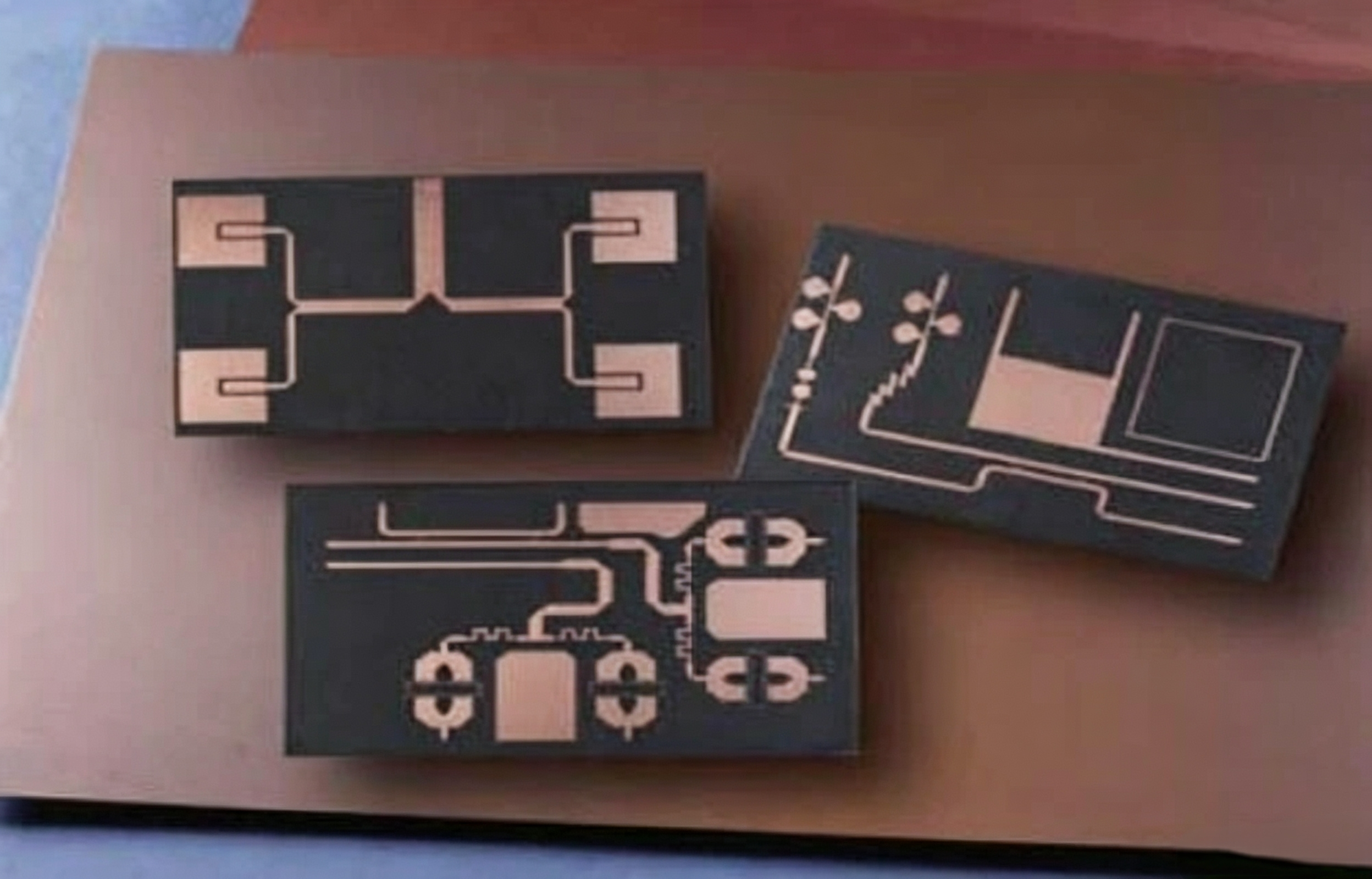
A high speed trace should run straight where it can, and where it has to turn it should turn gently. A right angle corner is a local widening of the conductor and therefore a small impedance discontinuity, and a sharp inner corner is also a place where the etchant behaves differently during fabrication. Two forty five degree segments or a smooth arc avoid both problems.
Length matching is the other geometric concern. Where several lines of a bus have to arrive together, the shorter ones are extended, usually with a serpentine. The tuning has to respect the spacing rules so that the added length does not create coupling, and it should be placed where there is room rather than squeezed into the last millimetre before the device.
Spacing And Crosstalk
Two traces running close together exchange energy through the capacitance and inductance between them, and the amount depends on how far apart they are relative to the dielectric thickness. The familiar three times the trace width rule is a way of expressing that relationship, and it is a starting point rather than a guarantee.
Crosstalk is worst where a victim line is quiet and a neighbour is switching, and where the two run parallel for a long distance. The design responses are to increase the separation where the layout allows, to reduce the parallel length, and to place a ground trace or a plane between aggressor and victim where the coupling is severe. The spacing rules for coupled traces are worth understanding in terms of the mechanism rather than as fixed numbers.

Stubs, Branches And The Via Stub
A branch from a signal line acts as a stub, and a stub reflects energy back toward the source. The most common example is a termination resistor placed at the end of a short spur, or a test point added on a long line. The electrical length of the stub is what matters, and keeping it short relative to the rise time of the signal limits the damage.
The via is a special case of the same problem. A through via carrying a signal from the top layer to an inner layer leaves an unused length of barrel below the exit point, and that length is a via stub. At frequencies where the stub approaches a quarter of a wavelength it presents a strong notch in the response. Back drilling removes it, and blind vias avoid it altogether, which is one of the reasons via selection belongs in the stackup decision rather than at the end of layout.
Impedance Continuity
The impedance of a trace depends on its width and on the distance to the reference plane, and both of those change at a pad, a connector or a transition between layers. Keeping the value constant means controlling the environment along the whole path, not just along the straight sections where the calculation was done.
The return path belongs to the same discussion. The current that flows out along a trace comes back through the plane beneath it, and it follows the path of least impedance, which at high frequency means directly underneath the trace. Anything that interrupts that plane, whether a slot, a cut out or a row of densely packed via antipads, forces the return current to divert. The diversion changes the impedance of the line above and radiates, which is why planning the ground and power structure is a layout task rather than an afterthought.
Differential Signalling
A differential pair carries its information in the difference between two conductors, which is why the pair has to be symmetrical. Equal width, equal spacing and equal environment along the length are what produce the intended differential impedance and what keep the common mode component small.
The pair should be treated as one object during routing. Placing a via or a component between the two traces breaks the symmetry, and any component inserted in series with a pair, such as a coupling capacitor, has to be small and placed symmetrically. Where a pair changes layers, the two vias should be treated as a matched transition with their own return vias.
Building The Skill
The areas above are learnable, and the fastest way to learn them is to connect each rule to the mechanism behind it and then to measure something. Reading a simulation of a net with a stub, then removing the stub and simulating again, teaches more than memorising a length limit. The same applies to crosstalk, to a plane split and to a via transition.
It also helps to work with a fabricator who will discuss the stackup. The impedance the design assumes has to be the impedance the shop can build, and that conversation is where a designer learns what is possible. gopcb supports controlled impedance and high speed designs with documented stackups, and the fabrication questions are usually answered during layout rather than after release.
FAQ
Do I need to simulate every net? No. Identify the nets with fast edges and long paths, simulate those, and apply the geometric rules to the rest.
Is the three times width rule always correct? It is a useful starting point. The amount of coupling depends on the dielectric thickness as well, so the rule has to be interpreted rather than applied blindly.
When is back drilling justified? When the via stub is long enough that its resonance falls inside the band of interest. Below that, the extra process step adds cost without benefit.