PCB Audio Circuit Layout: Keeping Analog Quiet
Audio is usually the last subsystem to receive attention on a dense board and the first that a user notices. A receiver that hisses, a headphone output that clicks when the radio transmits or a speaker that distorts at high volume are layout symptoms rather than component failures.
Why Audio Is Vulnerable
An audio signal occupies the same band as the noise that digital and switching circuits produce, and its amplitude is small. A few millivolts of coupling that would be invisible on a logic line is audible as a click, a hum or a background hiss at the output.
The ear is sensitive to structure rather than only to level. A steady hiss is tolerated, while a burst that repeats with the display refresh or the radio frame rate is immediately obvious, which is why the layout of the interfering source matters as much as the audio path itself.
Partition the Board by Function
The first decision is the floor plan. Analog audio, digital processing and radio belong in separate regions, and the boundaries should follow the signal flow rather than the convenience of component placement. Keeping the audio front end near its connector helps as well.
Where the product is small, complete separation is not possible, so the next best approach is to keep the sensitive nodes short and away from the noisy ones. A microphone input that runs across the board beside a switching supply will pick up noise however good the amplifier is.
Differential Inputs and Star Ground
An audio stage with a differential input rejects common mode noise that a single ended input accepts, so it is worth using wherever the source and the amplifier both support it. The two traces must then be routed together and matched in length.
Ground arrangement matters equally. A power amplifier draws large current pulses, and if those pulses share a ground path with a low level stage, the resulting voltage appears in series with the signal, which is the classic source of distortion and crosstalk.
Ground Currents and Return Paths
The rule for audio is to give each large current its own return path and to bring the references together at one point. A star arrangement at the input of the amplifier keeps the return current of the speaker out of the sensitive signal ground.
Digital returns are the opposite case: they should follow the trace that carries the signal rather than be diverted to a star point. Interrupting the natural return of a digital line increases the loop area and turns the trace into a better antenna.
Flooding and Local Shielding
Unused copper filled with ground and stitched with vias provides a low impedance reference and a measure of shielding between regions. The flood keeps the field of a trace local, and the stitching keeps the return path continuous where a signal changes layer.
Flooding is not a substitute for distance. A ground pour next to a noisy node reduces coupling but does not remove it, and a pour that is split into islands by a careless outline can make the return path longer rather than shorter.
Trace Length and Coupling
Analog audio should not be routed as a long single ended trace. A conductor that travels the length of the board absorbs whatever field the digital and radio sections produce, and the noise then arrives at the amplifier with the same gain as the wanted signal.
Where a long run cannot be avoided, the trace should be as short as possible, referenced to a solid plane, and separated from switching nodes by distance and, where the design allows, by a grounded guard conductor beside it.
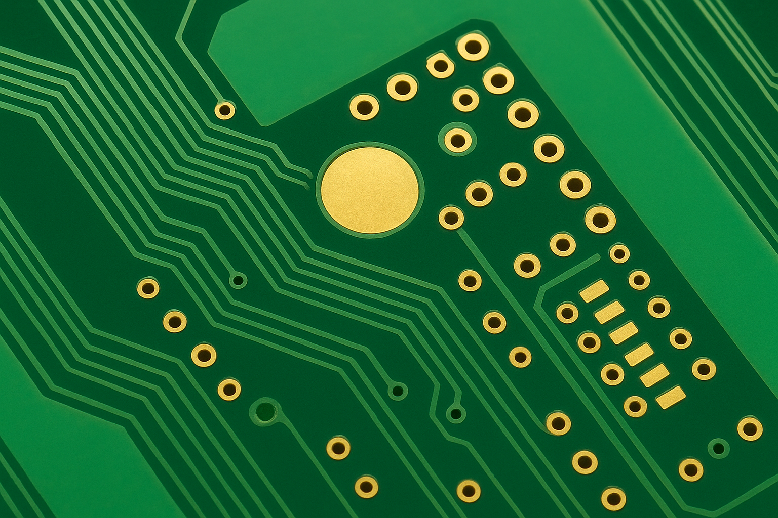
Component Placement Details
Feedback components belong next to the amplifier rather than on the far side of the board, because the loop they form sets the bandwidth and picks up noise. Decoupling capacitors belong at the pin they serve, with the return via placed beside the pad.
Input coupling capacitors should be placed before the most exposed part of the trace, so that the high impedance node is as short as it can be. A high impedance node is the most sensitive point in the circuit and should be treated as such in the floor plan.
Power and Decoupling
An audio rail has to be quiet as well as accurate. A regulator placed near the amplifier, followed by a small series element and local capacitance, keeps the supply impedance low across the audio band and reduces coupling between stages.
Where the amplifier shares a rail with digital circuits, the supply rejection of the amplifier sets the limit, and the layout can help by keeping digital current loops away from the analog rail and returning them towards the source of the disturbance.
Measuring What the Layout Achieved
Audio performance is measured rather than assumed. A listening test finds obvious faults, but a spectrum measurement with the digital section active shows the discrete tones that the layout allowed through, and those tones are what a customer complaint is usually about.
Comparing a measurement taken with the radio idle against one taken during transmission separates the sources. That comparison is far more useful than a single figure on a datasheet, because it identifies which section of the board needs the next change.
Mistakes That Cause Most Noise
Mixing analog and digital grounds at several points, routing audio across a switching node, using a long unshielded single ended input and leaving a high impedance node exposed account for most of the noise found in production.
None of these is expensive to avoid at the layout stage and all are expensive to correct later, because the cure usually means a new board revision rather than a change of value on one component.
Reviewing the Layout Before Release
An audio review should ask a small number of questions: where are the return currents of the largest loads, which nodes are high impedance, how far is the most sensitive trace from the switching node, and what happens when the radio transmits.
Answering them on the screen costs an afternoon. Discovering the same answers from a failed electromagnetic compatibility test costs a revision, and discovering them from a product return costs the reputation of the design.
The Connector and Cable Interface
The audio circuit should meet its connector at the edge of the board rather than in the middle of it, so that the sensitive conductors are short and the cable shield can be bonded to the chassis where it enters. A connector placed deep inside the board forces the input to travel through the noisiest part of the layout.
The ground of the connector and the ground of the analog region should meet at that point, and not at several points along the path. Where a jack also carries a switch contact, the return of that contact belongs with the analog reference rather than with the digital plane beside it.
When the Board Is Very Small
Handheld products leave no room for a clean partition, so the designer has to rely on distance, orientation and the reference plane. Placing the audio front end on the opposite side of the board from the switching regulator, with a ground plane between them, is often enough.
A small board also has less copper to spread heat and fewer vias to stitch a return path, so the audio ground needs to be planned as carefully as the signal. Treating the analog region as a distinct area of the plane, joined at one point, preserves the separation even when the components are close together.
FAQ
Does audio need its own ground plane? A separate analog region referenced to the same plane is normally enough, provided the return currents are kept apart and joined at a single point.
Should audio traces be shielded? Distance and a solid reference plane do most of the work. A shield is a last resort where the routing cannot be separated. The pour decisions are covered under copper flooding.
Why does noise appear only when the radio transmits? Because the coupling path is the radio field rather than a shared ground. Ground routing addresses the second case, while the first needs distance and filtering, as described in the guidance on mixed signal design.