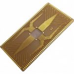
Alumina Ceramic Substrate Fabrication Step By Step
An alumina ceramic substrate is made in a sequence that has more in common with a chemical process than with printed circuit fabrication. The conductor is not etched from a copper foil; it is printed from a metal paste onto a green ceramic sheet, and the ceramic and the metal are fired together. The result is a hard, thermally stable board that carries power devices and high frequency circuits where a polymer laminate would not survive.
Each step in the sequence sets a constraint on the next, and understanding the flow makes it easier to see why a design rule for a ceramic substrate differs from the equivalent rule on an FR4 board. The sections below follow the process from powder to finished part.
Tape Casting And The Slurry
The process starts with a slurry of alumina powder, a binder, a plasticiser and a solvent. Tape casting spreads that slurry under a doctor blade onto a moving carrier film, and the solvent evaporates to leave a flexible sheet known as green tape. The thickness of the sheet is set by the gap under the blade and by the solids content of the slurry, and it is commonly between 0.1 and 1 millimetre.
The powder has to be well dispersed. A slurry with agglomerates produces a tape with density variations that survive firing as voids or as camber, and the dimensional tolerance of the finished part depends on the consistency of the green sheet. The binder provides the green strength that allows the tape to be handled, punched and laminated without tearing, so its content is balanced between flexibility and the amount of material that later has to be burned out.
Binder Burnout And Green Machining
Before the ceramic densifies, the organic content has to be removed. Burnout is a slow ramp through the temperature range where the binder decomposes, and it is run in air so that the products of decomposition can escape. A ramp that is too fast traps carbon inside the body, and residual carbon changes the colour, the insulation resistance and the dielectric loss of the fired part.
Green machining covers the operations performed while the tape is still flexible. Sheets are cut to size, stacked in the required number of layers, and laminated under heat and pressure to form a single body. Vias are punched mechanically or cut with a laser, and the accuracy of the punching sets the registration that every subsequent printing step has to work within. A punch that drifts by 50 micrometres produces a via that is offset from the pad printed over it.
Via Formation And Screen Printing
Vias are filled with a metal paste, usually tungsten or molybdenum, because those metals survive the firing temperature. Screen printing forces the paste through the openings in a patterned mesh, and the same technique prints the conductor pattern on the surface of each layer. The paste is a mixture of metal powder, a binder and a solvent, and its rheology determines how well the printed line holds its shape before drying.
Registration between layers is the critical parameter. Each printed layer must align with the vias in the sheet beneath it, and the accumulation of small errors across a stack is what limits how many layers a given process can produce reliably. A conductor printed with a fine pitch needs a finer mesh, a thinner emulsion and tighter process control, which is why high density ceramic substrates carry a cost premium.
Cofiring The Metallization
Cofiring is the step that gives the process its name. The laminated stack, with its printed conductors and filled vias, is fired at a temperature high enough to densify the alumina, typically between 1500 and 1600 degrees Celsius. During the same firing the metal paste sinters and bonds to the ceramic, and the two shrink together. Because the shrinkage is shared, the dimensional change of the part is significant and has to be compensated in the artwork.
The firing atmosphere depends on the metal. Tungsten and molybdenum require a reducing atmosphere, usually a wet hydrogen and nitrogen mixture, to prevent oxidation. The profile must also keep the shrinkage of the ceramic and the metal matched at every point in the ramp. A mismatch that develops during the ramp leaves the conductor under stress, and the result is a cambered part or a cracked metallisation that passes a visual check and fails in thermal cycling.
Plating And Finishing The Conductors
The fired metal is not solderable as it stands, so it is plated. A typical finish is a nickel barrier followed by gold, applied over the tungsten or molybdenum pads. The nickel provides a diffusion barrier and the gold provides a surface that resists oxidation and wets reliably. The plating has to be thick enough to be continuous and thin enough to avoid stress, and the process window is narrower than on a copper pad.
Where a component is attached directly to the ceramic, the pad geometry is designed for the die or the lead frame rather than for a standard footprint. This is where the design rules of a ceramic substrate diverge most sharply from those of a laminate. The layout and the process are closely linked, which is why the fabrication sequence and the requirements for a multilayer prototype are worth reviewing before the artwork is released.
Inspection And Where Yield Is Lost
Inspection of a fired ceramic substrate looks for camber, for vias that are not filled, for metallisation that has lifted, and for dimensional drift outside tolerance. Camber is measured across the whole part and is the parameter most likely to stop an assembly line, because a substrate that is not flat will not sit on a placement table or on a heat sink. Dimensional drift is compared against the shrinkage predicted from the artwork.
Most yield loss comes from a small number of causes: a punch that has drifted, a printed layer that is out of registration with the via beneath it, and a firing profile that has changed with the load in the furnace. Because the parts are fired in batches, a problem introduced in the furnace affects the whole load, and it is usually detected after the fact. Tracking the firing profile with each load is the cheapest protection against repeating it.
Additional Considerations for This Build
Practical attention to via metallization pays for itself here, because it decides whether the finished board behaves as the drawing intended. Where the requirement is not stated on the fabrication drawing or in the assembly notes, the shop has to assume a default, and that default is rarely the value the design was simulated with. Stating via metallization explicitly, together with the tolerance that applies, removes the assumption and keeps the result predictable from batch to batch.
Process Control and Verification
On a design of this kind, cofiring is the item that decides how the rest of the board is arranged. Keeping a sample from the panel turns a dispute into a measurement, because the same coupon can be re-examined by both parties without rebuilding the batch. Reviewing the design before the data is released is cheaper than correcting it after the panel is in the tank, because every step downstream inherits the decision made at the front end.
Related reading: our fabrication notes, board quality and design release notes cover the same ground.
FAQ
Why is tungsten used instead of copper for ceramic conductors? Copper melts below the temperature needed to densify alumina. Tungsten and molybdenum survive the firing and bond to the ceramic, and they are plated afterwards to become solderable.
How much does the part shrink during firing? Shrinkage depends on the powder and the process, but a figure around 15 to 20 percent linear is typical. It is characterised for the process and compensated in the artwork.
Can vias be added after firing? Not easily. Vias are punched in the green tape and filled with paste before lamination. A via that escapes those steps cannot be formed in the fired ceramic.