Plasma Treatment for PCB Surface Activation Before Coating
Conformal coating and adhesive bonding both depend on a surface that the material can wet. A board that has passed through soldering, cleaning and handling carries an invisible layer of contamination that prevents that wetting, and the coating that looks continuous may be sitting on top of a weak interface. Plasma treatment addresses that problem directly by modifying the surface rather than washing it. This guide explains how gopcb uses plasma for surface activation and how the result is verified.
Why Surfaces Need Preparation
Every surface exposed to air collects a layer of adsorbed material: water, hydrocarbons and residues from flux, handling and packaging. That layer has a low surface energy, which means a coating or adhesive applied to it beads up rather than spreading. The interface that forms is weak even when the coating appears uniform.
The problem is invisible in normal light, which is why it survives inspection. A board can look perfectly clean and still fail a wetting test, and the resulting adhesion failure may not appear until thermal cycling or humidity exposure has stressed the interface. Preparation is therefore a process step, not a cleaning gesture.
What Plasma Treatment Does
Plasma is an ionised gas containing ions, electrons and reactive species. When it contacts a surface, two things happen: organic contamination is etched away and chemical groups are attached to the surface. Both effects raise surface energy, and they act only on the outermost molecular layers.
Because the treatment is limited to the surface, it does not change bulk properties, dimensions or electrical behaviour. That is its main advantage over abrasive or chemical preparation methods, which either remove material or leave their own residue behind.
<img src="https://www.gopcba.com/wp-content/uploads/2026/08/24-layer-pcb-1536×640-1.webp" alt="Contact angle measurement confirming surface energy after plasma treatment” />
Surface Energy and Wetting
Surface energy is measured in millinewtons per metre and describes how strongly a liquid is attracted to a solid. A high energy surface pulls a coating flat and thin, while a low energy surface causes it to pull back into droplets. Plasma treatment raises surface energy by adding polar groups such as hydroxyl and carboxyl.
The effect is large and immediate. A treated polyimide or FR-4 surface can move from a low energy state that repels coating to a high energy state that wets readily, and the change is confined to a depth of nanometres, so nothing about the board is structurally altered.
Contact Angle Measurement
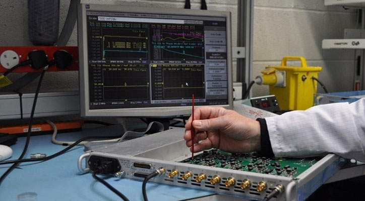
Contact angle is the practical way to measure the result. A drop of a known liquid is placed on the surface and the angle at its edge is measured. A low angle means the liquid spreads and the surface is wettable; a high angle means it beads and the surface is not ready.
The measurement is quick and can be done on a production sample rather than only in a laboratory. Water and diiodomethane are common test liquids, and the pair allows both the polar and dispersive components of surface energy to be calculated, which is more informative than a single angle reading.
Adhesion Improvement for Coatings
Adhesion depends on intimate contact at the molecular level, and that requires wetting. A conformal coating applied to a properly activated surface flows into the microscopic texture of the laminate, and the mechanical key plus the chemical bonding produces an interface that resists peeling and thermal stress.
The improvement is most visible in the failure mode. A poorly prepared surface fails at the interface between coating and board, leaving a clean separation. A well prepared surface fails within the coating itself or in the laminate, which shows that the interface was stronger than the materials around it.
Plasma in PCB Fabrication Steps
Plasma is used in several places beyond coating preparation. It removes drilling smear from via walls before plating, it desmears and etches back laminate in sequential lamination, and it activates surfaces before adhesive bonding in flexible circuits. Each application uses different gas chemistry and process conditions.
In assembly, the treatment is normally placed immediately before coating or underfill dispensing, because the activated surface relaxes over time. Our notes on flexible PCB processing describe how the same principle applies to adhesive bonding on flex substrates.
Process Parameters and Control
Gas mixture, power, pressure and treatment time together determine the result. Oxygen plasma is aggressive at removing organics, argon provides physical bombardment, and mixtures including hydrogen or nitrogen are chosen for specific surface chemistries. Power and time control how much material is removed as well as how much is activated.
Over-treatment is a real risk. Excessive power or time can etch the laminate, expose glass fibres and create a surface that is chemically active but mechanically rough. The process window should be established experimentally and then controlled, because the difference between an activated surface and a damaged one can be a few minutes of exposure.
Limitations and Risks
Plasma is a line of sight or diffusion limited process depending on the system. Vacuum plasma treats all exposed surfaces but requires a batch chamber, while atmospheric plasma can be integrated inline but reaches into recesses less effectively. Shadowed areas under components may remain untreated.
The activated surface also ages. Polar groups reorient or become covered by airborne contamination, and the wettability gain decays over hours or days depending on storage. That is why the treatment should be placed as close as possible to the coating step and why a maximum delay should be written into the process. Our fabrication notes checklist covers how such limits are documented.
Verifying the Result
Verification combines a surface measurement and a functional test. Contact angle or surface energy measurement confirms that the treatment worked, while a coating adhesion test, such as a cross hatch or peel test on a sample, confirms that the improvement translates into a real bond.
Both should be done on production parts at intervals, not only during process development. Where a coating is applied for reliability in a humid or high voltage application, the adhesion result is the evidence that the coating will perform, which is the same kind of functional evidence used when PCB quality is assessed.
Process Control and Verification
On a design of this kind, plasma treatment is the item that decides how the rest of the board is arranged. Reviewing the design before the data is released is cheaper than correcting it after the panel is in the tank, because every step downstream inherits the decision made at the front end. Documenting the assumption is part of the design work, and a short note on the drawing prevents a question that would otherwise arrive a day later and cost a day of schedule.
FAQ
What does plasma treatment do to a PCB surface? It removes organic contamination and attaches polar chemical groups to the outermost layers, which raises surface energy. The higher energy allows coatings and adhesives to wet the surface and form a stronger interface.
How is plasma treatment verified? Contact angle measurement is the fastest check, because a low angle indicates a wettable surface. Adhesion testing on a coated sample confirms that the measured improvement produces a bond that survives peeling and thermal stress.
Does plasma treatment damage the board? Not when the process is controlled. Excessive power or treatment time can etch the laminate and expose glass fibres, so the window should be established experimentally and monitored, with the treatment placed immediately before coating to limit surface aging.