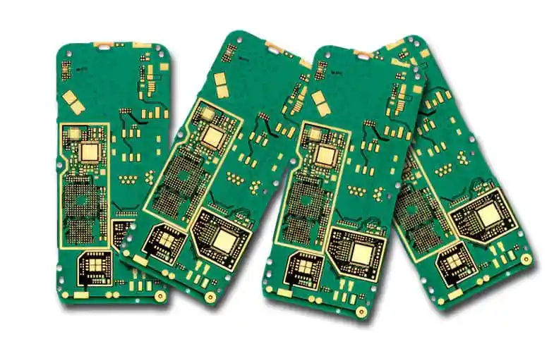
Single Sided vs Multilayer Flexible PCB: Process Differences
A single sided flexible circuit and a multilayer flexible circuit share the same materials but almost nothing about their processing. The first is essentially a patterned film with a coverlay; the second requires lamination cycles, plated through holes and layer registration, and each of those steps changes both the cost and the design rules.
What Separates the Two Constructions
A single sided flex has one conductor layer on a polyimide base, covered by a protective film with openings at the pads and component sites. It bends easily, weighs almost nothing and costs the least of any flexible construction.
\n
A multilayer flexible PCB stacks two or more conductor layers with adhesive or adhesiveless bonding, connects them with plated through holes and protects the outer surfaces with coverlay. The added capability comes with a process chain that resembles rigid board fabrication far more than film processing.
Single Sided Flex Processing
Processing begins with a copper-clad polyimide sheet. The circuit is imaged and etched, the coverlay is applied and cured under pressure, and the surface finish is deposited on the exposed pads. The outline is then cut, often by laser or die, and the parts are inspected.
There is no plating step, no drilling in the electrical sense and no lamination cycle beyond the coverlay bonding. That short sequence is why single sided flex has a short lead time and a low tooling cost, and why it remains the default for a simple interconnect.
Multilayer Flex Processing
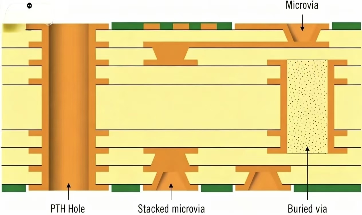
Multilayer processing adds two operations that dominate its cost and its yield. The first is lamination, which bonds the layers together under heat and pressure; the second is plating, which forms the barrels that connect them.
Each lamination cycle subjects the material to thermal excursion. Polyimide and its adhesives absorb moisture and expand, and the layers must be registered accurately both before and after the press, because the material moves during the cycle. Registration tolerance therefore has to be larger than on a rigid board of the same feature size.
Plated Through Holes in Flexible Material
Plating a hole in a flexible circuit is harder than in a rigid one. The material is thin and compliant, the hole walls are less rigid and the chemistry must penetrate a stack of bonded films without damaging the adhesive interfaces.
The result is that plated through holes in flex are more restricted in aspect ratio and more sensitive to process control. Where a connection between layers is needed only at a pad, a common alternative is a via-in-pad or a button-plated or riveted connection, depending on the reliability requirement.
<img src="https://www.gopcba.com/wp-content/uploads/2026/08/PCB-Box-Build-Assembly.jpg" alt="Plated through hole and coverlay on a multilayer flexible circuit” />
Layer Registration and Dimensional Stability
Polyimide moves more than glass-reinforced epoxy during processing, so every layer retains the possibility of shifting relative to its neighbours. The designer’s response is to allow larger annular rings and greater clearance between features on different layers than would be accepted on a rigid board.
Panel design also matters. Placing the circuits on a carrier frame maintains position through the process and keeps the thin material flat, and the frame is removed only after lamination and plating are complete.
Coverlay, Adhesive and Stiffeners
Coverlay selection is the same for both constructions, but the consequences differ. On a multilayer board the coverlay must bond to a surface that has already been through lamination, and its cure cycle adds another thermal excursion to the stack.
Stiffeners are bonded in the same way and must be placed outside the bend regions. Where components are mounted, a stiffener is effectively mandatory, and its thermal expansion relative to the flexible substrate determines whether the solder joints survive cycling.
Cost Structure and Volume
The cost differences are large. A single sided flex is priced mostly on material and on the area processed, while a multilayer flex is priced on the number of lamination and plating cycles, the registration difficulty and the yield loss at each step.
That bias means the crossover is rarely about electrical necessity alone. A design that can meet its requirements with two single sided circuits and a connector is often cheaper than one multilayer circuit, even when the multilayer version is electrically tidier.
Design Rules and Bending
Bending behaviour differs between the two. A single sided circuit bends easily because it has one conductor layer, and the copper is thin. A multilayer circuit has neutral-axis considerations: the layers on the inside of the bend compress and those on the outside stretch, so the copper placement relative to the neutral axis determines the fatigue life.
Design rules respond by limiting dynamic bending to constructions with a well-defined neutral axis, and by recommending that a multilayer flex be used for static bends only where possible. Where the circuit must flex repeatedly, a single sided design with the conductor on the neutral axis is the more reliable choice, and the guidance on flexible interconnect selection covers the alternatives.
Choosing Between Them
Choose single sided flex when the interconnect is simple, the bend is gentle or static and the volume justifies a modest tooling cost. Choose a multilayer flexible PCB when the routing cannot fit on one layer, when shielding or controlled impedance is required, or when the assembly must include components on both sides.
In every case, confirm the fabrication sequence with the supplier before releasing artwork, since registration allowance and bend limits depend on the specific process. Reviewing design and fabrication conventions for flexible constructions at the start of the layout is cheaper than correcting them later.
Testing and Inspection Differences
Test access differs between the two constructions. A single sided flexible circuit can be probed at its pads and its integrity verified visually, but there is no barrel to inspect because there is no plating. Where a connection between sides is achieved by a rivet or a soldered wire, its quality is verified by pull or resistance measurement rather than by cross section.
A multilayer flexible board is inspected much like a rigid board: coupons for registration, microsections for barrel quality and electrical test for continuity. The difference is the handling, because the sample is thin and compliant, and sectioning it requires mounting in resin so that the layers remain aligned during polishing.
Both constructions need a functional bend test rather than a visual check, since the failure mode is fatigue at the conductor rather than an obvious defect. A fixture that flexes the part through the specified radius and monitors resistance is the only practical way to confirm the design before it reaches production.
FAQ
Is a multilayer flexible PCB always more expensive? Per unit area, generally yes, because of the additional lamination and plating cycles. Total cost can still favour it when it replaces several single sided circuits and their connectors.
Can a multilayer flex be bent dynamically? It can be designed to, but the fatigue life depends on the position of the copper relative to the neutral axis and on the radius. A single sided construction is usually the safer choice for a high cycle count.
Why do flexible boards need larger annular rings? Because polyimide moves during lamination and plating more than a rigid laminate does. The larger ring is the allowance that keeps the hole inside the pad after the material has shifted, and see pad design standards for the geometry involved.