System Level PCB Design in the Modern Project
A modern board project mixes hardware and software, several power domains and a radio, and the design decisions are made before either discipline has finished. The layout has become the place where those decisions are reconciled rather than the last step of a hardware task.
Why the Flow Changed
The change came from the packages. Area array devices with hundreds of connections replaced parts with leads on a pitch a human could route, and the density of the escape routing became a design problem in its own right.
At the same time the clock frequencies rose, so the delay of a trace became a significant part of the timing budget. What used to be a drawing exercise became an electrical one, and the two had to be done together.
Partitioning Before Layout
The first serious decision is how the system divides into hardware blocks. A partition that is settled early gives each block a defined boundary, a defined interface and a defined set of signals that cross it.
Getting this wrong produces loops: a change in one block forces a change in another, and the two revisions invalidate each other. Spending time on the block diagram before the schematic is complete is usually cheaper than redrawing the board.
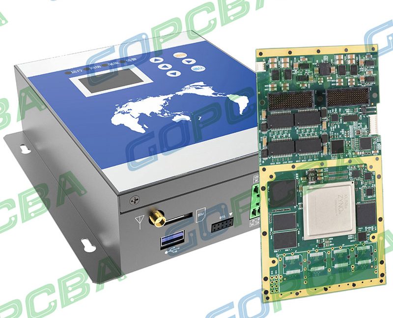
<img src="https://www.gopcba.com/wp-content/uploads/2026/05/smart-energy-PCBA-1.jpg" alt="System block diagram and PCB layout of a mixed signal board” />
Mixed Signal Reality
A modern product is rarely purely digital. The same board carries a processor, a switching supply, an analog front end and a radio, and each of those has a different relationship with the reference plane and with the return currents.
The design problem is the interaction, not the individual blocks. A converter that is perfectly laid out in isolation will still disturb a sensor if the two share a ground path, and mixed signal practice exists to make that interaction predictable.
Packages and Routing Density
A package with a fine pitch has fewer routing channels between adjacent balls than the designer needs, which is why escape routing is planned before the placement is fixed. The number of layers follows from that plan rather than the other way round.
Where the density exceeds what a conventional through via can serve, the design moves to blind and buried vias, to a via in pad construction or to a higher layer count. Each of those choices affects cost, lead time and manufacturability.

Timing and Signal Integrity
Once the rise time of a signal is short compared with the length of the trace, the trace has to be treated as a transmission line. The delay, the impedance and the return path all become part of the timing budget.
This is where the older design flow fails. A tool that checks connectivity and clearance but knows nothing about the impedance or the delay will pass a board that cannot work, and the designer will not discover it until the hardware is built.
Power Integrity
The supply network is now a design subject of its own. The impedance of the path from the regulator to the die has to be low across a band of frequencies that extends far beyond the switching frequency, and that requirement is met by a combination of planes, capacitors and placement.
A decoupling capacitor that is placed on the far side of the board is a component in a circuit that the designer never intended to build. The placement and the via arrangement are as important as the value, and both are decided in the layout.
The Role of the Tools
The design tools have followed the same path. Constraint driven layout, impedance aware routing, and analysis integrated into the editor are now standard, and the schematic has become the source of constraints rather than only of connectivity.
That integration changes the workflow: the constraints are entered with the schematic and checked continuously, so the review at the end is about the decisions rather than about the data entry errors that a late check would have found.
Working With Software
The firmware team needs the board early and will make changes that affect the hardware. Pin assignments, bus widths and the memory map are shared, and a design that treats them as a fixed hardware decision will be revised more often than it should.
Keeping the interface definitions in one document and reviewing them before the layout is frozen removes most of that churn. The development process for an assembly can then follow a plan rather than a series of surprises.
Prototype and Production
The first build answers the electrical questions, and everything after it answers the manufacturing ones. Layer count, finish, panelisation and test coverage are usually revisited once the design works, because the cost of producing it becomes the dominant consideration.
That is not a failure of the design process. It is the natural point at which the product stops being a prototype, and the earlier the manufacturing review happens the less it costs to accommodate.
What to Document
The block diagram, the interface definitions, the stackup, the constraints and the test plan belong in one place. Each of them is used by a different person during the project, and each of them changes.
A change log that records why a constraint exists is worth as much as the constraint itself. The next engineer will otherwise optimise away a rule whose purpose is not visible, and the problem the rule prevented will return on the next revision.
Additional Considerations for This Build
Practical attention to system level pays for itself here, because it decides whether the finished board behaves as the drawing intended. Where the requirement is not stated on the fabrication drawing or in the assembly notes, the shop has to assume a default, and that default is rarely the value the design was simulated with. Stating system level explicitly, together with the tolerance that applies, removes the assumption and keeps the result predictable from batch to batch.
Process Control and Verification
On a design of this kind, power integrity is the item that decides how the rest of the board is arranged. Where the requirement is not written down, the shop supplies its own default, and the default is chosen for the process rather than for the design. The measurements that matter are the repeatable ones: conductor width and spacing, annular ring, finished hole size, plating thickness and surface finish are all verifiable on a coupon that travels with the panel.
Running a first article through the same checks as the production panel confirms that the two agree, and that comparison is the cheapest form of process control available at prototype stage. Keeping a sample from the panel turns a dispute into a measurement, because the same coupon can be re-examined by both parties without rebuilding the batch.
FAQ
Why is the partition decided so early? Because every interface that crosses a block boundary becomes a constraint, and constraints that arrive late force the layout to be redone.
When does a trace become a transmission line? When its length is a significant fraction of the rise time of the signal. The exact ratio depends on the margin the design carries.
Do fine pitch packages always mean more layers? Often, but escape routing and via technology can sometimes keep the count down. The decision should be made after the fanout is planned.