Ceramic Substrate Technology Trends For Power
Ceramic substrates sit at the point where a circuit has to be electrically insulating, dimensionally stable and thermally conductive at the same time. Polymer laminates can satisfy the first two requirements and struggle with the third, which is why the ceramic option appears in power modules, radio frequency circuits and packages where the device itself generates a high heat flux.
The material has moved from a niche into the mainstream as wide bandgap semiconductors have entered production. This article looks at where the technology stands, what aluminium nitride changes, and what the trend means for a designer choosing a substrate.
Ceramic Substrates In Modern Electronics
The useful properties of a technical ceramic come from its structure: a dense, inorganic body with a high melting point, a low dielectric loss and a thermal expansion close to that of silicon. Those properties do not degrade with temperature in the way a polymer does, so the material holds its dimensions through a soldering cycle and through the thermal cycling of a power application.
The disadvantage is cost and processing. A ceramic substrate is made in a sequence of casting, printing, lamination and firing, and it cannot be produced in the panel sizes and the volumes that a laminate can. The decision to use one is therefore driven by a requirement that no laminate can meet, and the rest of the design follows from there.
The choice among ceramic materials is therefore a set of trade offs rather than a ranking. Alumina offers the best mechanical strength and the lowest cost, aluminium nitride offers the best thermal conductivity, and beryllium oxide offers more again but is restricted because its dust is toxic. Silicon nitride sits between the others, with a high strength and an expansion close to that of silicon, which makes it attractive where thermal cycling is severe.
For a designer the relevant question is which property is limiting. Where the limit is the heat flux through a small area, the thermal conductivity decides. Where the limit is the number of cycles before the interface cracks, the expansion match decides. Where the limit is the dielectric withstand, the thickness and the quality of the ceramic decide, and the material itself is secondary.
Aluminium Nitride And Thermal Conductivity
Alumina is the workhorse material, and it is chosen for its dielectric strength, its mechanical strength and its cost. Its thermal conductivity is several times that of a polymer laminate but still modest compared with metals. Aluminium nitride is the material that changed the picture, with a thermal conductivity several times higher than alumina while remaining an electrical insulator.
The importance of that figure is the heat flux it permits. A wide bandgap device can dissipate a large power in a small area, and the substrate has to carry that flux away without a temperature difference that would destroy the device. Where alumina would allow the junction to overheat, aluminium nitride keeps the rise within the limit, and the module can be run at its rated current.
Substrates For Power Modules
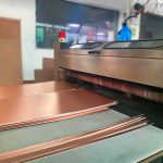
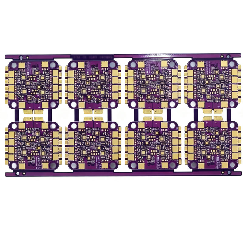
A power module combines several devices on one substrate, with the substrate providing electrical insulation, thermal conduction and the interconnections between the devices. Two constructions dominate. The direct bonded copper approach bonds a copper sheet to each face of a ceramic tile, and the pattern is etched from the copper. The cofired approach prints the conductors onto a green ceramic and fires the assembly, which allows vias and multiple layers but requires the shrinkage to be managed.
Both depend on the bond between the metal and the ceramic surviving thermal cycling. The two materials expand at different rates, and the interface carries the resulting shear stress with every cycle. Aluminium nitride has a thermal expansion closer to that of copper than alumina does, which is one reason it has become the preferred material for the higher power modules.
MLCC And Electronic Ceramics
The same material family appears in the multilayer ceramic capacitor, which is the component that decouples almost every supply on every board. The demand for smaller bodies with higher capacitance and a higher operating voltage pushes the ceramic formulation toward thinner dielectric layers and more precise stacking, and the manufacturing tolerances that can be held in that stack determine the voltage rating of the finished part.
For a board designer the practical effect of that trend is a change in what the component datasheet says about the de rating of the capacitance under bias and over temperature. A capacitor that is smaller for the same nominal value is not necessarily interchangeable, because the dielectric formulation changes with the size class. The substitution has to be checked against the actual operating conditions rather than against the nominal value.
Electric Vehicles And Wide Bandgap Devices
The largest driver of ceramic substrate volume is the electric vehicle, where the traction inverter, the on board charger and the direct current converter all use power devices that are run hard. Silicon carbide and gallium nitride devices switch faster and run hotter than silicon, and the substrate has to carry the heat and withstand the higher electric field that the faster switching produces.
That combination is what makes the ceramic substrate a system level decision rather than a component one. The insulation has to withstand the field, the thermal path has to handle the dissipation, and the expansion has to match the device so that the interface survives the cycles. When the substrate is chosen late in the project, one of the three usually has to be compromised, and the compromise shows up as a thermal or a reliability problem in qualification.
What This Means For Board Designers
The trend matters even for designers who will never specify a ceramic substrate, because the components they place are being built to tighter thermal and voltage limits. A power device in a smaller package has a higher heat flux, and the copper on the board has to spread that heat. A capacitor with a thinner dielectric has a stronger voltage coefficient, and the effective capacitance under bias is lower than the nominal value.
The response is to work from the operating conditions rather than from the nominal ratings, and to size the copper and the decoupling from a measurement or a calculation. The tools for doing that on a laminate board are the familiar ones, and the reasoning about multilayer prototypes, the splitting of power planes and the general fabrication route still applies. What changes is the margin, and it is smaller than it was.
FAQ
Is aluminium nitride always better than alumina? It has a much higher thermal conductivity, but it also costs more and is harder to machine. Alumina remains the right choice where the thermal requirement is moderate.
Can a ceramic substrate be replaced with a metal core board? Sometimes, where the requirement is thermal rather than dielectric, but a metal core board cannot provide the same electrical isolation or the same dimensional stability at high temperature.
Does a smaller MLCC have the same effective capacitance? Not necessarily. Thinner dielectric layers change the voltage and temperature coefficients, so the effective capacitance under bias can be lower than that of a larger part with the same nominal value.