ENIG Process Control: Electroless Nickel Immersion Gold
Electroless nickel immersion gold is the finish of choice for fine pitch, for wire bonding and for boards that will be stored for a long time before assembly. It is also the finish with the narrowest process window, because the nickel layer is deposited by a chemical reaction that has to be controlled across the whole panel surface, and the gold layer that follows is thin enough that a small variation changes the soldering behaviour. This article covers the control points that decide whether the finish is reliable, from the nickel bath through the immersion step to the thickness and solderability checks.
Why ENIG Is Chosen
The finish gives a flat surface, which matters for fine pitch printing and for the placement of area array packages. The nickel provides a hard diffusion barrier and the gold protects the nickel from oxidation, so the surface remains solderable after months of storage.
It is also one of the few finishes that is compatible with both soldering and wire bonding. That combination is what makes it attractive for a mixed assembly, and it is also what makes the process control demanding, because the surface has to satisfy two different sets of requirements at the same time. The abbreviation ENIG is used so often that the two layers behind it are forgotten, and that is exactly where the process risk sits.
The Two Layers and What Each Does
The nickel layer is the structural part of the finish. It provides the barrier that stops the copper and the tin from diffusing into each other, and it gives the gold a surface to sit on. Its thickness, its phosphorus content and its structure all affect the soldering behaviour.
The gold layer protects the nickel during storage and dissolves into the solder during reflow. It is intentionally thin, because a thick gold layer would form brittle intermetallics in the joint. Our surface finish guide compares how the different finishes behave in the same applications.

Nickel Bath Control
The nickel bath is a chemical reduction process, and the deposition rate depends on the temperature, the pH, the concentration of the reducing agent and the age of the bath. The reaction also produces hydrogen and by products that accumulate, so the bath has to be analysed and maintained rather than merely topped up. Bath turnover is a slow variable, and the analysis interval should be short enough that a drift is caught before a panel is processed in a marginal bath.
The pH is the parameter that most often drifts unnoticed, because it changes as the reaction proceeds and as boards are processed. A pH at the edge of the window produces a deposit with a different phosphorus content, and the phosphorus content is what determines how the layer behaves during soldering.
Immersion Gold and Its Limits
The gold is deposited by an immersion reaction that stops when the surface is covered, which is why the layer is thin and self limiting. The process also attacks the nickel underneath while it is running, so the time and the temperature have to be controlled to avoid excessive corrosion of the nickel surface.
An over long immersion step produces a nickel surface that is rough and corroded, and the gold that covers it is not a continuous protection. That condition appears later as a soldering defect or as a black pad failure. Because the gold thickness is self limiting, the corrosion is governed by the time and the temperature rather than by the deposit.
The Corrosion Mechanism Behind Black Pad
Black pad is the failure where the nickel surface under the gold has been corroded, leaving a layer that the solder cannot wet. In a section it appears as a dark, irregular interface, and in assembly it appears as a joint that does not form or that fractures with very little force.
The mechanism is associated with an over aggressive immersion gold step, with a nickel deposit that is more susceptible to corrosion because of its phosphorus content, and with contamination of the nickel surface before the gold. All three are process control issues rather than material defects.
Surface Preparation Before Nickel
The copper surface has to be clean and active before it enters the nickel bath, because the deposition is a chemical reaction that starts on the catalytic surface. Residue from the previous steps, oxide or handling contamination produces areas where the nickel does not deposit or deposits poorly.
Those areas appear as a thin or missing nickel layer under a normal looking gold surface. The preparation sequence therefore has to be controlled with the same care as the plating bath itself, and the queue time between the preparation and the bath should be defined. The activation step that precedes the nickel bath is the one that most often explains a localised deposition problem. Our solderability guide covers how the finished surface is verified.
Thickness Targets and Measurement
The nickel thickness is specified as a minimum and the gold as a range, because the two have different roles. A nickel layer that is too thin does not act as a barrier, while a gold layer that is too thick produces brittle intermetallics in the joint.
Thickness is measured by X-ray fluorescence on a coupon or on the panel, and the measurement should be taken at several locations because the deposition varies across the panel. A single reading is not a statement about the distribution across the panel. Our plating thickness guide covers the measurement practice for the plated layers.
Soldering Behaviour and Intermetallic Growth
The gold dissolves into the molten solder within seconds and the joint that forms is between the solder and the nickel. The intermetallic layer that grows at that interface is what carries the joint, and its growth continues during subsequent thermal cycles.
A joint with a well formed intermetallic layer is reliable, while one with an irregular layer fails under stress. A joint that has been reworked several times carries a thicker intermetallic layer and fails differently from one that has seen a single reflow. The finish is therefore not only a shelf life decision but also a joint reliability decision.
Process Monitoring and Documentation
The monitoring plan should include the bath analysis, the pH, the temperature, the immersion time, the thickness measurements and the solderability test result. The combination is what makes a defect traceable to a bath condition rather than to a supplier. Those records should be linked to the lots produced on the bath rather than filed by date alone.
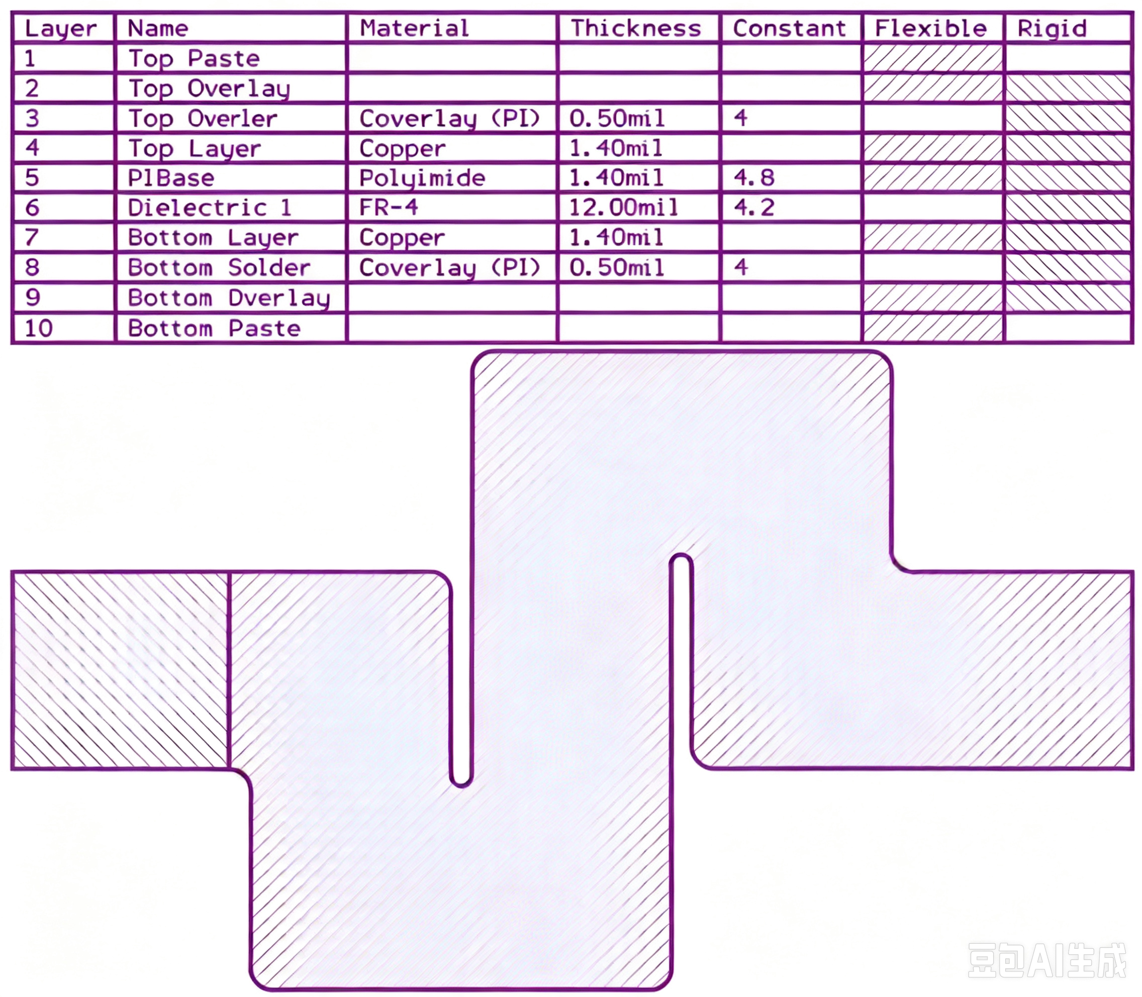
At gopcb the finish is recorded with the stack up for each design and the acceptance is judged in our quality documentation, so that a change in the bath history can be linked to a change in the boards it produced.
FAQ
How thick should the gold layer be? It is normally a thin layer measured in fractions of a micrometre, enough to protect the nickel and thin enough to dissolve completely during reflow. A thicker layer is not an improvement.
Can black pad be detected before assembly? It can be indicated by a solderability test and confirmed by a section, but a board that looks normal can still be affected. The more effective control is the bath history and the immersion step parameters.
Is ENIG suitable for wire bonding? It is, and that is one of the reasons it is selected. The bonding behaviour depends on the nickel and the gold thickness and on the absence of contamination on the surface.