Via in Pad for BGA Fanout: Process and Design Points
A via in pad places the connection directly in the centre of a surface mount land instead of beside it. On a fine pitch ball grid array the pads are already close together and the escape routing between them is the first thing to run out of room, so moving the via into the pad recovers a channel on every row and can remove a layer from the stackup. The trade is process complexity rather than a loss of electrical performance.
The decision belongs to the layout and the fabrication house together. A via in pad that is open, unfilled or poorly capped will drain paste during reflow and leave a void under the ball, and no amount of inspection afterwards will repair that joint. What follows is what the design has to specify and what the fabricator has to hold.
When Fanout Space Runs Out
The classic escape pattern for a ball grid array drops a short trace from each pad and then a via just outside the ball field. That works while the pitch allows a trace between two pads. Below roughly 0.5 mm the traces have to be thinner and the vias larger relative to the gap, and at some point the arithmetic simply fails: there is not enough room for a pad, a track and a via in the space between two balls.
The usual symptom is a design that demands an extra pair of layers purely to escape the device. Once the via moves into the pad, the escape channel disappears and the same device can often be routed on a shallower stackup, which is where much of the cost saving of this approach actually comes from, whether that is an any layer HDI build or a simpler sequential laminate.
How the Via Is Filled and Capped
A filled via is drilled and plated like any other, and the difference starts afterwards. The barrel has to be closed with a material that survives assembly and keeps the pad flat. Conductive paste, non conductive epoxy and copper plating are the three routes, and each one changes what the board can do next and how flat the finished surface will be.
Resin plugging followed by planarisation and copper capping is the most common answer for a pad that has to be soldered. The paste is forced into the barrel from one side, cured, and then ground back so that the resin sits inside the hole rather than on top of it. The cap is then plated over the pad so that the solder sees copper.
Plating and Planarity Requirements
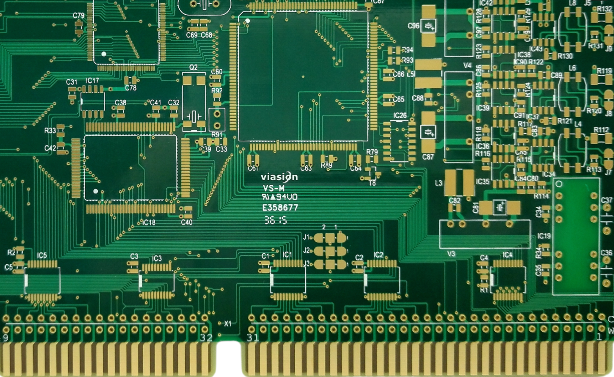
A plated over via is the only version that behaves exactly like a solid pad, because the copper that the paste wets is continuous with the pad around it. Achieving that continuity is the hard part: the resin has to be recessed slightly below the pad surface before plating, otherwise the cap sits proud and the paste deposit on that land is thicker than on its neighbours.
The specification that matters is flatness, expressed as a tolerance across the pad rather than as an average. A dimple in the middle of the pad reduces the paste volume, while a proud cap lifts the ball. Both show up later as a joint that looks acceptable on X-ray but fails after thermal cycling, so the requirement belongs in the fabrication notes with an explicit number attached to it.
Stackup and Drill Considerations
Via in pad is usually paired with a stacked or staggered microvia arrangement, and the choice between them decides how many lamination cycles the board needs. Stacked vias give the shortest path and the smallest keep out area but demand very tight layer to layer registration, which is where the difference between a capable shop and a cheap one becomes visible in the yield rather than in the quotation.
Aspect ratio is the other constraint. A small drill through a thick board produces a barrel that is difficult to fill completely, and trapped chemistry inside a partially filled hole will outgas during reflow. Where the thickness or the drill size pushes the ratio past what the process can fill reliably, the honest answer is to change the stackup or the drill rather than to accept a partly filled HDI structure.
Soldering over a Filled Via
Paste volume on the affected lands has to be recalculated once the via is filled, because the hole no longer swallows part of the deposit. Stencil apertures that were opened up to compensate for a through hole now over print, and the excess can bridge to the neighbouring ball on a pitch that has very little room to spare.
The measurement that closes the loop is the paste volume on the via in pad lands compared with the ordinary ones on the same device. If they differ, the first article is the place to correct it. The wider checks on the finished assembly follow the same logic as any other first article, as described in the guide to yield and quality control.
Cost, Yield and When Not to Use It
Every filled via adds steps: an extra drill and plating pass, plugging, curing, grinding and capping. On a board where only a handful of the ball field actually needs the technique, applying it everywhere raises the price for no benefit, and the cheaper answer is to use it only on the inner rows that cannot escape any other way.
It is also worth asking whether the via has to be in the pad at all. Where the density permits a short dog bone escape, the conventional approach has fewer process steps, better yield and no risk of a dimple under a ball. The technique is a tool for a specific density problem, not a default choice for every ball grid array design.
Reviewing the arrangement before release is cheap. Moving a via, widening a land or adding a layer at the layout stage costs nothing compared with a fabrication re-spin, which is the point made in the checklist for a layout review.
Additional Considerations for This Build
Practical attention to BGA fanout pays for itself here, because it decides whether the finished board behaves as the drawing intended. Where the requirement is not stated on the fabrication drawing or in the assembly notes, the shop has to assume a default, and that default is rarely the value the design was simulated with. Stating BGA fanout explicitly, together with the tolerance that applies, removes the assumption and keeps the result predictable from batch to batch.
Deliberate attention to HDI stackup pays for itself here, because it decides whether the finished board behaves as the drawing intended. Where the requirement is not stated on the fabrication drawing or in the assembly notes, the shop has to assume a default, and that default is rarely the value the design was simulated with. Stating HDI stackup explicitly, together with the tolerance that applies, removes the assumption and keeps the result predictable from batch to batch.
Process Control and Verification
On a design of this kind, via in pad is the item that decides how the rest of the board is arranged. A stack-up that is drawn rather than described removes most of the ambiguity from a quotation, and it lets the fabricator price the board against the dielectric and copper weights that will actually be used. Where the requirement is not written down, the shop supplies its own default, and the default is chosen for the process rather than for the design.
FAQ
Does a via in pad always need a filled barrel? Yes if it sits under a soldered land. An unfilled hole wicks paste away from the joint during reflow and leaves a void that thermal cycling will open up.
Can a filled via be reworked? Not in the usual sense. The plug is buried under the pad, so any repair of a ball on that land disturbs the cap and the joint has to be considered suspect afterwards.
Is the technique limited to HDI boards? No, but it is most often combined with microvias. The plugging and capping steps are the same on a conventional multilayer board, where the drill is simply larger.