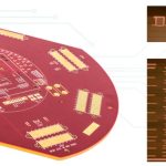
Thermal Via: Design Rules and Process Limits
A power device does not lose its heat to the air. It conducts it into the copper pad beneath it, and from there into the planes and the other side of the board, where a heatsink or an airflow can remove it. On a surface mount package with a thermal pad, an array of small vias under the pad is the bridge between the surface copper and the rest of the board, and the design of that array decides how hot the junction runs.
This article explains the thermal path, how the resistance of a via is estimated, how the array is arranged, and how the vias are filled and verified.
The Thermal Path And Its Resistances
Heat travels from the die to the case, then through the solder joint into the copper pad, then through the vias into the internal planes, and finally sideways through the board to the edges, the other surface, and the air or the heatsink. Each of those steps has a resistance, and the largest one is often not the via array but the lateral spreading resistance, because a one ounce copper plane conducts heat well in a straight line and poorly across a distance.
That is why a copper area larger than the package footprint is worth more than a few extra vias. The pad spreads the heat out of the device, the vias move it through the thickness of the board, and the plane under the array spreads it again so that a larger area of the board can dissipate it. A design that places vias under a pad but keeps the pad small throttles the path before the vias are reached.

Estimating What A Via Contributes
The plated copper in a via is a thin tube rather than a solid rod. A via of three tenths of a millimetre with twenty five micrometres of plating carries a copper cross section that is a small fraction of the hole area, and its thermal resistance is roughly a hundred degrees per watt for a board of standard thickness. That figure is an order of magnitude rather than a precise value, because it depends on the drill diameter, the plating thickness, the board thickness, and whether the via is filled with copper or with a polymer.
The consequence is that a single via does very little and the array does the work. Ten vias in parallel bring the resistance of the thickness path to about ten degrees per watt, which is comparable to the spreading resistance that surrounds them. Beyond a certain number the array stops helping, because the heat has to reach the vias in the first place, and adding more holes only removes copper from the pad that was spreading the heat.
Arranging The Array
The vias belong under the thermal pad, spread across its area at a regular pitch rather than clustered at the centre. A cluster in the middle leaves the corners of the pad with a long lateral path, while a grid that reaches the edges lets the whole pad collect heat and pass it through. The pitch is limited by the drill and by the solder mask web between the holes, and by the requirement that the pad remains flat enough for the component to sit on it.
The vias should connect to a plane rather than to a trace, because a trace has a small cross section and a long path. Where the package ground is also the thermal path, the plane is the same net, and the design then has to keep that plane continuous under the device rather than split it into islands. The rules for dividing planes between rails are described under power plane splitting, and the choice between a filled via and an open one under via in pad or plated through.

Filling And Capping
An open via inside a solder pad is a defect rather than a feature. During reflow the paste wicks into the hole, which leaves the joint starved and creates a void at exactly the point where the heat has to pass, and the solder that has entered the hole may appear on the other side of the board as a bump or a short. The via must therefore be filled and the surface planarised before the component is placed.
The common methods are copper filling followed by plating, which gives the best thermal path and a surface that can be plated over, and polymer filling followed by a copper cap, which is cheaper and adequate for many designs but has a lower conductivity. A via that is tented on the opposite side and left open on the pad side is not a solution, because the solder still has somewhere to go. Where the via array is large, the total volume of the holes is significant, and the paste deposit has to be increased or a solder preform added so that the joint is not starved after the vias have taken their share.
Assembly And The Joint
The joint under a thermal pad is where most of the thermal budget is lost in practice. A solder void reduces the conducting area and creates a local hot spot, and the void percentage is usually controlled by X-ray inspection against a limit written for the product. The solder volume, the paste pattern, the reflow profile, and the flatness of the pad all influence the result, and a board that warps through the reflow peak will produce a joint that is thin on one side and voided on the other.
The interface material above the device belongs to the same thermal path, and its resistance is often larger than the via array. A package that is clamped to a heatsink with a poorly chosen interface will run hot no matter how many vias sit under it, so the array and the interface should be designed together rather than in separate documents.
Verification
Three measurements support the design. A thermal simulation gives the expected junction temperature and shows where the resistance is concentrated. A measurement on a real assembly, with a thermocouple or an infrared camera on the case and a known power dissipation, gives the actual resistance of the whole path. A cross section of the via fill confirms that the holes are filled and capped as specified, and an X-ray of the joint shows the voiding under the pad.
When the measured case temperature is well above the prediction, the usual causes are a voided joint, a via array that is smaller than the drawing, an unfilled via that swallowed the paste, or a plane that is not continuous under the device. Each of those is visible in an inspection step, which is why the thermal design of a board is verified with a section and a radiograph rather than with a calculation alone. The fabrication context is described under PCB design and fabrication.
FAQ
How many thermal vias are enough? There is no fixed number. The array resistance falls with every via added, but the spreading resistance in the pad and the plane sets a floor, and beyond that point extra holes remove copper without helping.
Can the vias be left open? Not under a solder pad. Solder wicks into an open hole and starves the joint, which creates a void exactly where the heat must pass. The vias have to be filled and capped or planarised.
Does a filled via conduct better than a polymer filled one? A copper filled and plated via conducts better and gives a flatter surface, while a polymer filled via with a copper cap is cheaper and adequate for moderate power. The choice follows the required thermal resistance.