Thermal Simulation And CFD For PCB Designs
A thermal simulation predicts how hot a circuit will run before the board exists. It answers two questions that a calculation on a datasheet cannot: how much of the heat leaves through the copper rather than through the package, and how much the neighbouring components raise the local temperature. The value of the exercise is not the absolute number that comes out of the model, which is never better than its inputs, but the comparison between design options that it makes possible.
This article explains what is modelled, how the board and the components are simplified, how the boundary conditions dominate the result, and how the model is verified.
What The Simulation Solves
The CFD model solves for the temperature field in the board, the air around it, and the packages on it, using conduction in the solids, convection at the surfaces, and radiation where the temperatures are high. The output is a set of temperatures: the junction temperature of each device, the temperature of the copper plane, the air temperature inside the enclosure, and the velocity field of the air if the convection is modelled rather than assumed.
The interesting output for a board designer is usually the copper temperature rather than the junction temperature, because the copper carries the current and its temperature limits the trace width. The rules for sizing a trace from its temperature rise and its current are described under trace width and current calculation, and the simulation provides the local ambient that those rules assume.
The transient case is a separate question from the steady state one. A device that dissipates a watt continuously reaches a temperature that a steady state model predicts, while a device that dissipates ten watts for a millisecond is limited by the heat capacity of the copper around it rather than by the convection at the surface. A transient model uses the same geometry with the thermal mass of the copper included, and it is the appropriate tool for a pulsed load, a motor driver, or any circuit where the peak dissipation is much higher than the average.
Simplifying The Board And The Components
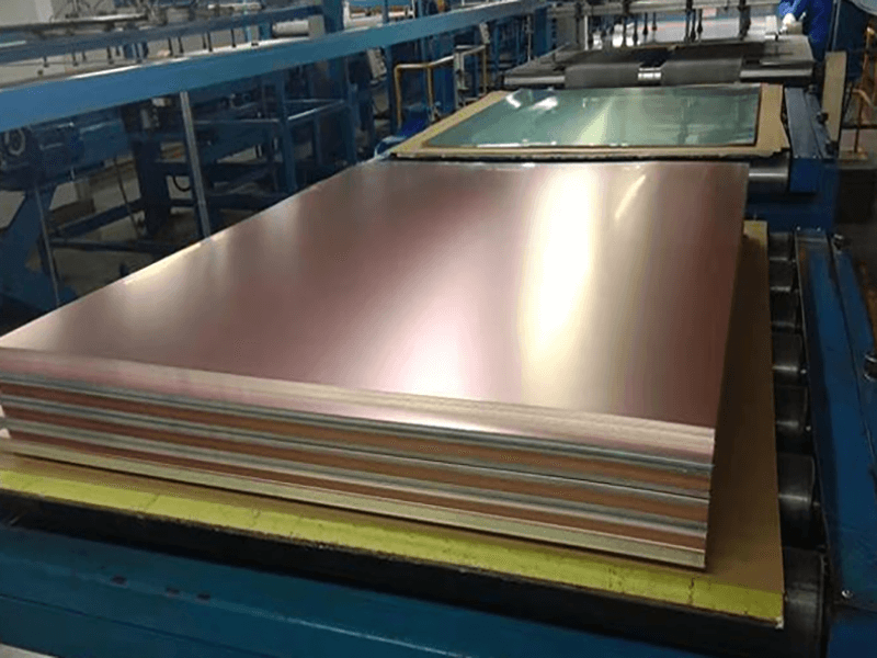
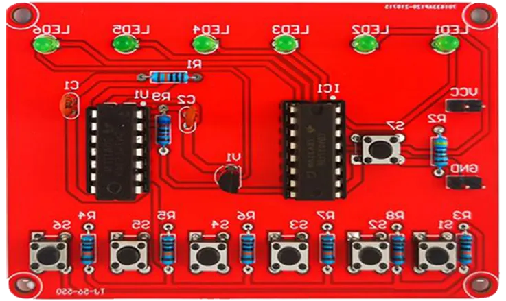
A detailed model with every trace would be far too large to solve, so the board is usually represented as a block with anisotropic conductivity: a high value in the plane of the board, which represents the copper, and a low value through the thickness, which represents the resin. The two values come from the copper fraction of each layer and from the laminate properties, and they are the parameters that change the result the most. The in plane value is set by the copper conductivity of the layer and the through plane value by the resin, and both are inputs to the model rather than results from it, because in-plane conduction is the main path by which heat spreads away from a device.
The components are simplified in a similar way. A device is represented as a block with a defined power dissipation and a thermal connection to the board through its pads or its thermal pad, or as a two resistor network using the junction to case and junction to board resistances from the datasheet. The simplifications are acceptable when the question is comparative, and they are least reliable when the package has an internal structure that dominates its thermal path, such as a large exposed pad or an internal heat spreader.
Boundary Conditions Dominate The Result
The boundary conditions are the weakest part of any thermal model. The convection coefficient at a surface depends on the airflow, on the geometry, and on the orientation, and a natural convection coefficient may be five or ten watts per square metre kelvin while a forced flow at a few metres per second raises it by an order of magnitude. A model that assumes still air in an enclosure that will actually be ventilated predicts a temperature that is far too high, and one that assumes a fan where the product is sealed predicts a temperature that is far too low.
The environment inside an enclosure is the other dominant input. A board in a sealed plastic box heats the air around it, and the internal ambient may be twenty degrees above the outside, which changes every downstream calculation. The way the planes are arranged, and where the copper is continuous, is described under power plane splitting. The heat sink, the interface material, the mounting hardware, and the cabinet airflow all belong in the model, and leaving one of them out is the most common way to produce a number that is confidently wrong.
Reading The Results
A junction temperature is compared with the maximum rated value with a derating margin, not with the absolute limit, because the model has an uncertainty and because the production unit will not be identical to the model. The local copper temperature is compared with the value the trace sizing assumed, which is the check that the electrical and thermal designs are consistent.
The distribution is as informative as the maximum. A hot spot in the middle of a plane indicates a spreading problem, a large gradient between two sides of a board indicates an asymmetric stack, and a package that is hotter than its neighbour with the same power indicates a blocked conduction path rather than a higher dissipation. Those patterns point to a specific change, which is what makes the model useful even when its absolute accuracy is limited.
Verifying The Model
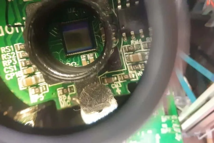
A model is verified by measurement on a real board. Thermocouples attached to the case or to the copper, an infrared camera under a low emissivity coating, or a thermal test die that reports its own temperature all give a measured value that can be compared with the prediction. The difference between the two is usually in the range of ten to twenty percent, and the calibration is done by adjusting the convection coefficient and the board conductivity until the model reproduces the measurement.
The calibrated model is then used to compare options, which is where its value lies. If a change reduces the predicted temperature by ten degrees, that comparison is likely to hold even if the absolute value is uncertain, because the same uncertainty applies to both cases. Simulation is therefore a design tool for ranking options, and a measurement is the evidence that the final option works. The fabrication side of the same decisions is described under PCB design and fabrication.
Where to draw the line is a matter of complexity. A single device on a generously sized board can be estimated from the datasheet junction to ambient resistance with an allowance for the copper area, and a full model adds little. A board with several power devices, a constrained enclosure, and a requirement to keep every junction below a limit needs a three dimensional CFD model with a real convection solution, because the interactions between the devices and the enclosure decide the result.
Additional Considerations for This Build
Practical attention to CFD pays for itself here, because it decides whether the finished board behaves as the drawing intended. Where the requirement is not stated on the fabrication drawing or in the assembly notes, the shop has to assume a default, and that default is rarely the value the design was simulated with. Stating CFD explicitly, together with the tolerance that applies, removes the assumption and keeps the result predictable from batch to batch.
Deliberate attention to copper conductivity pays for itself here, because it decides whether the finished board behaves as the drawing intended. Where the requirement is not stated on the fabrication drawing or in the assembly notes, the shop has to assume a default, and that default is rarely the value the design was simulated with. Stating copper conductivity explicitly, together with the tolerance that applies, removes the assumption and keeps the result predictable from batch to batch.
Process Control and Verification
On a design of this kind, copper conductivity is the item that decides how the rest of the board is arranged. Running a first article through the same checks as the production panel confirms that the two agree, and that comparison is the cheapest form of process control available at prototype stage. Keeping a sample from the panel turns a dispute into a measurement, because the same coupon can be re-examined by both parties without rebuilding the batch.
Related reading: our fabrication notes, board quality and design release notes cover the same ground.
A first article check confirms that the process and the drawing agree on the points listed above, and that the coupon data supports the values used in the design.