Common PCB Design Mistakes That Delay Projects
Most boards that miss their schedule are not defeated by difficult technology. They are delayed by a handful of avoidable errors that were present in the data when it was released. Cataloguing common PCB design mistakes is therefore not an academic exercise: each one has a specific check that removes it, and the checks take minutes when they are part of the release routine.
Errors That Start in the Schematic
Schematic errors propagate silently. A wrong pin assignment, an inverted enable polarity or a missing pull-up produces a layout that is electrically correct and functionally wrong. These defects survive design rule checking because they are not rule violations. They appear only when the first article is powered up.
The most effective countermeasure is a structured review that walks the schematic net by net against the datasheets. Pay particular attention to power pins, reset and enable polarities, and pins that must be tied high or low for a specific mode. Mark every pin whose state matters at reset, because those are the ones that produce confusing intermittent behavior when they are wrong.
Footprint Errors and Library Discipline
Footprint errors are the second largest source of rework. A pad spacing measured from a drawing instead of from the recommended land pattern, a pin numbering that follows the symbol rather than the package, or a courtyard that omits the connector mating envelope all cause assembly problems that no electrical test can detect.
Build a controlled library and verify each new footprint against the manufacturer’s land pattern before it is used. A printed one-to-one plot compared with the physical part takes two minutes and catches the majority of footprint defects. Where a component is expensive or has a long lead time, order a sample and place it on the plot before releasing the design.
Netlist, Connectivity and Test Point Gaps
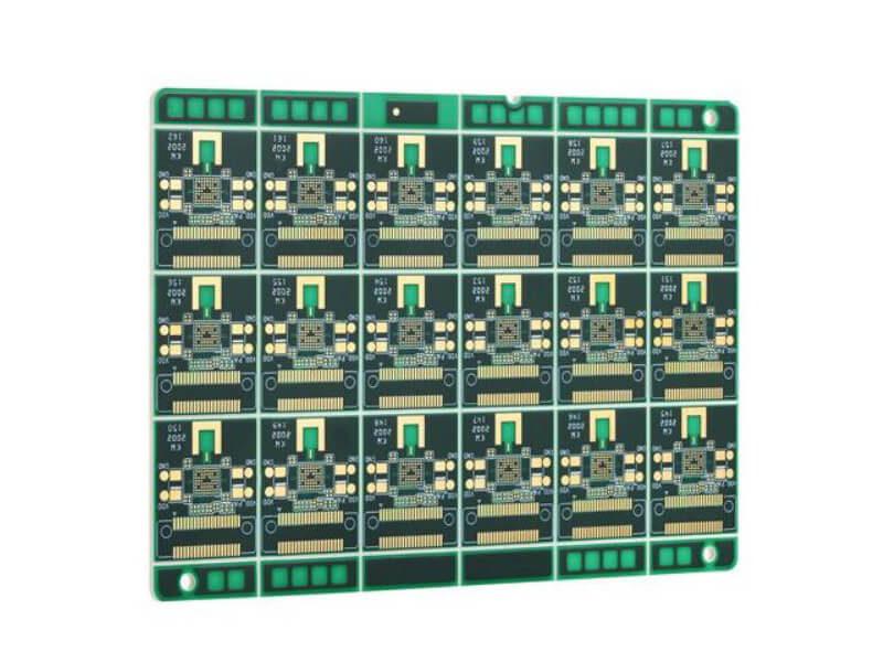
Netlist mismatches occur when the layout database and the schematic drift apart, usually after a late change is made on one side only. Always regenerate the netlist before routing and compare the result with the previous revision. Layout tools can highlight the differences, but only if the comparison is actually run.
Test point coverage is a related omission. A board with no access to the rails, to reset or to the programming interface cannot be debugged efficiently. Reserve pads for the supplies, the reference clocks and the boot configuration, and keep them clear of components so a probe can reach them. The cost is a few square millimeters; the benefit is measured in days of debugging.
Design Rule Check Misuse
A design rule check is only as good as the rule set behind it. Running a check with the tool defaults often reports hundreds of warnings, most of them irrelevant, and the reviewer learns to ignore the report. The opposite mistake is worse: tightening the rules until the report is clean by waiving everything that mattered.
Set the rules from the fabrication drawing, run the check, and then read every remaining violation before waiving it. Record the reason for each waiver and the person who approved it. A clean report with a documented waiver list is a stronger release artifact than a report that was never examined.
Mechanical and Enclosure Conflicts
Mechanical conflicts are expensive because they are discovered late, when the enclosure already exists. Connector heights, cable bend space, screw head clearance and the keep-out area around sensors are all defined by the mechanical design, and they must appear on the layout as exact constraints rather than as approximate notes.
Import the mechanical outline into the layout tool and route against it. Check the component height map against the enclosure, including the tallest capacitor, the programming header and any heatsink. A board that fits but cannot be assembled because a cable cannot reach is just as unusable as one that does not fit at all.

Bill of Materials and Documentation Gaps
The bill of materials is part of the design data, not a purchasing afterthought. Missing manufacturer part numbers, duplicated reference designators and footprints that disagree with the placement file all stop a build. So do notes that exist only in a conversation, such as a substitution agreed with the assembler and never written down.
Release the fabrication drawing, the assembly drawing, the bill of materials and the placement data as a single package, and check that all four describe the same revision. Most of the delays attributed to the factory are actually differences between documents that were released on different days.
Thermal and Current Oversights
Current and thermal mistakes are the ones that pass every test in the laboratory and fail in the field. A trace sized for the typical current rather than the peak, a thermal pad with too few vias, or a connector rated for the steady state but not the inrush current will work on a bench supply and fail in a sealed enclosure.
Size conductors from the worst case, confirm the connector and component ratings against the same number, and check the thermal path from the dissipating device to the ambient. Follow trace width and current calculation rather than a rule of thumb carried over from a lower power design.
Mask, Silkscreen and Manufacturability Details
Small documentation details cause disproportionate delays. A silkscreen legend that overlaps pads, a reference designator that is printed under a component, or a polarity mark that disappears after assembly all slow down inspection and repair. Keep silkscreen off exposed copper, size the text for the intended process, and place every designator where a technician can read it with the board installed.
Solder mask features deserve the same care. A dam narrower than the process can hold will lift or flake, and an opening that is too small for the pad pitch will bridge during assembly. Check the dam width against the fabricator’s standard, review the design against design guidelines for manufacturable boards, and confirm the surface finish choice suits the pitch and the volume.
Preventing Mistakes Systematically
A short release checklist built around solder mask dam width and the items above removes most of these defects: netlist comparison, footprint plot verification, rule check with documented waivers, mechanical fit check, thermal review and document version alignment. Six items, each taking minutes, and each catching a category of error that would otherwise cost days.
Keep the checklist in version control with the design, and update it whenever a new failure mode is found. gopcb reviews layout data before fabrication and can flag the mechanical, thermal and documentation gaps that most often interrupt a build, which turns the review into a shared responsibility rather than a single reviewer’s memory.
FAQ
What single check catches the most errors? Comparing the netlist from the layout against the current schematic, together with a one-to-one footprint plot. Together they catch the majority of defects that pass automated checks and appear only at bring-up.
Should every rule violation be fixed? No. Some are cosmetic or reflect a deliberate deviation, such as a wider trace inside a connector footprint. What matters is that each deviation is understood and recorded rather than ignored.
How much review is enough for a simple board? Even a two-layer design should receive a netlist comparison, a rule check and a fit check against the enclosure. The review scales with risk, but the three core checks apply to every board regardless of complexity.