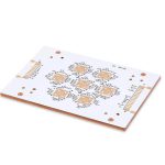
PCB Edge Plating Design Guide
A plated edge turns the side of a printed circuit board into a conductor. Copper is wrapped from the top surface around the profile and onto the bottom surface, so a module can be soldered by its side rather than by a pad on the face. The feature is easy to describe and fussy to build, because the plating has to survive the routing step.
What Edge Plating Is
PCB edge plating is a continuous copper layer on the board profile that connects the top and the bottom copper. It is used to give a ground connection to a chassis, to shield a module, or to provide a soldering surface along the side of the board.
The copper on the edge is the same material as the surface copper, and it usually carries the same finish. The layer is thin, often between twenty and thirty microns, so it is not a mechanical structure and should never be used as a bearing surface.
Because the edge is where the board is routed, the copper has to be deposited before the profile is cut. A shop that has not plated an edge before will route first and then try to plate, and the result is a partial wrap that looks acceptable in a photograph and fails in a thermal cycle.
Castellations and Half Holes
A castellation is a plated half hole on the board edge. The hole is drilled and plated in the normal way, then the profile is routed through the middle of the hole, leaving a semicircular plated feature that can be soldered to a pad on a mother board.
Castellations are common on radio modules and on power modules, where the module is placed flat and soldered around its edge. The solder fillet on the half hole carries both the current and the mechanical load, so the geometry of the half hole is a design decision rather than a manufacturing detail.
The drill diameter sets the width of the castellation and the plating follows the barrel, so a small hole gives a narrow feature that will not accept a fillet. A large hole weakens the edge of the board and reduces the number of castellations that will fit along a given length.
The relation between the hole and the finished feature is covered in the hole types guide, and it is worth reading before the module outline is fixed.

Process Sequence for a Plated Edge
The sequence matters more than any other factor. The hole is drilled and plated in the normal way, then the profile is routed with a tool that leaves the copper wrapped over the edge instead of cutting it away.
A common approach is to route the edge in two passes: a rough cut that leaves a small amount of material, then a finishing cut that trims to the final profile. The second cut is where the copper is formed over the edge, and its feed rate determines whether the wrap is smooth or torn.
The edge wrap comes from the surface plating, so the ductility of the deposit is what decides the result. A brittle deposit cracks at the corner, and the crack becomes a path for moisture and for a plating void. The plating thickness has to be specified on the drawing, not left to the shop.
Design Rules and Clearances
The edge copper has to be connected to a net, and that net should be a plane or a wide trace. A thin signal trace that runs to the edge is a mechanical risk, and it is also difficult to plate evenly because the current distribution in the plating bath is uneven near the profile.
Copper on layers that are not plated should be kept back from the edge, so that the router does not expose an internal layer. A component courtyard should stay clear of the edge by the routing tolerance plus a margin, otherwise a part may hang over the profile.
The profile tolerance and the copper acceptance are related, because a board that is routed large carries more copper over the edge and a board that is routed small carries less. The board outline tolerance should be agreed with the shop before the artwork is released.
Soldering and Assembly
Soldering to a plated edge requires a fillet that forms on the vertical face, which is a harder joint to make than a fillet on a flat pad. The heat has to reach the edge, and a large ground plane on the board will pull heat away from the joint while the solder is still solidifying.
The finish on the edge should match the finish on the pads so that one flux works everywhere. A gold finish gives a long shelf life but a weak fillet, while a tin finish solders easily and oxidises quickly. The surface finish and the assembly process should be chosen together.
For a castellation, the solder volume is the variable that decides the joint strength. Too little solder leaves a gap at the top of the half hole, and too much wicks into the module and shorts an adjacent castellation on a fine pitch part.
Inspection and Common Defects
The defects to look for are a partial wrap, a crack at the corner, a delaminated edge and a burr left by the router. Each has a different cause, and each is easier to catch on a coupon than on a finished assembly.
A burr along the profile is the most common complaint from assembly, because it lifts the board off the fixture and it can short against a metal housing. A light deburr after routing removes it, and the deburr has to be specified so the plating is not rubbed away at the same time.
The copper on the edge also has to be checked for a plating void where the wrap crosses the corner. A void there is a hidden open circuit that shows up only after the module has passed a thermal cycle, which is exactly the kind of fault that a coupon is meant to find.
Visual inspection at low magnification shows the wrap and the burr, while a cross section is needed to see the copper thickness on the vertical face. A cross section coupon is the only reliable way to prove the process before a production panel is built.
A delaminated edge usually points back to the laminate and to the routing parameters rather than to the plating, because the mechanical stress of the cut is what separates the layers. The fabrication notes should require a sample for approval on the first order.
FAQ
Can any board be edge plated? Almost any rigid board can be, provided the copper on the edge is connected to a net and the shop has the process. Thin boards and flex circuits need a different approach.
Is edge plating the same as a castellated module? Castellations are a specific form of edge plating in which half holes are soldered to a mother board. A plated edge can also be a continuous strip used for grounding rather than for soldering.
Does edge plating change the board outline tolerance? It does, because the copper wrap depends on the cut. The profile has to be held tighter than a plain board, and the shop should confirm the tolerance before the order is placed.