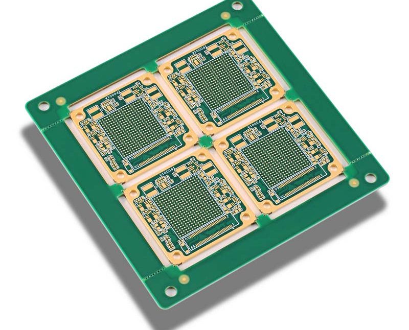
Board Outline, Slot and Tolerance Rules for PCB Fabrication
The mechanical side of a fabrication package is where designs are most often under-specified. The copper layers describe the circuit, but the outline, the slots, the tolerance and the flatness requirement have to be stated explicitly, and where they are not, the fabricator applies a default. Knowing what the defaults are and where they matter is the difference between a board that fits and a board that is returned.
Defining the Board Outline
The board outline belongs on a dedicated mechanical layer, and the convention should be stated so that the fabricator knows which layer to read. A separate keep-out layer is normally used to prevent routing, not to define the shape; using it for both purposes creates ambiguity about which geometry is a cut and which is a restriction. Where the design tool supports it, the outline and the internal cut-outs should be drawn on the same mechanical layer so that all of the physical geometry is in one place.
Slots and internal cut-outs are drawn as shapes on that layer rather than as drilled holes, unless the cut-out is a simple round hole. A long slot expressed as a series of overlapping drill hits produces a ragged edge and is difficult to control, while a routed slot produces a clean edge with a defined width. Our fabrication notes guidance explains how to record the layer mapping.
Outline Tolerance
Where the drawing does not state a tolerance, the practical default for the outline is a symmetric band of a few tenths of a millimetre. That default is adequate for a board that sits inside a housing with clearance, and inadequate for a board that locates against a mechanical datum, such as a module that plugs into a card cage or a board whose mounting holes align with a chassis.
Where the board position is determined by its edge, the tolerance has to be stated and it has to be achievable. A tighter requirement usually means that the board is routed rather than punched, and that the tooling is dedicated to the design. Stating the requirement with the order allows the fabricator to select the process rather than adapting one afterwards.

Flatness and Warpage
Flatness is specified as a maximum deviation relative to the board diagonal, and it matters most for boards that go through automated assembly, where a board that is not flat will not sit correctly on the conveyor or the placement table. The requirement is affected by the stack-up, the copper distribution and the lamination process, so it should be reviewed alongside the layer design rather than treated as a separate inspection item.
A warpage specification that is tighter than the design can support will not be met consistently, no matter how it is inspected. Where a design needs a flatter board, the route to it is a balanced stack-up and a symmetric copper distribution, which is where the problem originates.

Drill, Annular Ring and Aspect Ratio
The mechanical data also defines the holes. A via should normally be specified with a finished inner diameter above about 0.3 millimetres and an outer diameter above about 0.6 millimetres for general-purpose work, with a component pad at least fifty per cent larger in diameter than the finished hole. A small drill has a mechanical limit: a nominal 0.3 millimetre tool produces a finished hole slightly smaller, and the smallest available drill sets the floor for the whole design.
The annular ring, the copper remaining around a hole after the drill and the registration tolerance are accounted for, is the clearance that prevents an inner layer connection from being cut. The aspect ratio, the board thickness divided by the hole diameter, determines how reliably the hole can be plated. Both should be checked against the specified process before the design is released, because both are difficult to change afterwards.
Line Width Tolerance and Copper Weight
Conductor width is produced to a tolerance rather than exactly, and a figure of around plus or minus twenty per cent is a realistic expectation for a standard process. A design that assumes the nominal width at both the minimum and maximum current case will be optimistic in one of the two. The same applies to spacing, where the tolerance reduces the isolation on the narrow side.
Copper weight interacts with this. A heavier copper foil requires a wider minimum line and spacing, so the achievable density falls as the copper thickness rises. Where a design needs both heavy copper and fine features, the two requirements have to be reconciled before the artwork is generated.
Bringing the Mechanical Data Together
The practical checklist is short: state the layer that defines the outline, state the outline tolerance and the flatness requirement, define slots and cut-outs as geometry rather than as drill hits, list the minimum via and annular ring dimensions for the process, and state the conductor width tolerance. Our design release checklist covers these items, the copper balance material explains where warpage comes from, and the aspect ratio notes describe how plating capability follows the hole geometry.
Fabrication Allowances the Design Should Assume
A fabricator will make small adjustments to a design in order to produce it. Pad diameters are sometimes enlarged on a single-sided board to improve solderability, conductor widths and pad rings are sometimes compensated to allow for etching, and spacing that falls below the process limit is widened where the design can tolerate it. Those adjustments are normal, but they should not be relied on: a design that assumes the fabricator will correct a violation has no guarantee that the correction will match the intent.
The design-side counterpart is to leave the allowance explicitly. Specify the minimum line width and spacing that the process supports for the copper weight being used, allow for the width tolerance in the current calculation, and keep the annular ring above the registration requirement rather than at it. The design then has margin that the fabricator can consume without changing the electrical behaviour.
FAQ
Which layer should carry the board outline? A dedicated mechanical layer, used consistently for the outline and for internal cut-outs. The important thing is not which name the layer has but that the fabricator knows which one defines the physical shape, and that the same layer is not also used for routing restrictions. That information belongs in the fabrication notes.
Why does a long slot cost more than a series of holes? Because a routed slot is a milling operation with a defined cutter path, whereas overlapping drill hits are a compromise that produces a rough edge and is harder to control dimensionally. A design that needs a clean slot with a controlled width should ask for it as a routed feature, and accept the tooling that goes with it.
What does gopcb check in the mechanical data? We check that the outline is unambiguous, that the slots and cut-outs are defined as geometry, that the via dimensions and the annular ring are inside the process capability for the specified thickness, and that the tolerance and flatness requirements are achievable. These are the items that determine whether the finished board fits the assembly, and they are cheapest to correct before the data is released.