Controlled Impedance: Design Rules and Process Limits
Controlled impedance is a specification that a board must meet, not a property that a stackup automatically provides. The difference between a nominal value and a delivered value comes from the tolerance of every parameter in the stackup: trace width, dielectric thickness, dielectric constant and copper thickness. Specifying the target without specifying the tolerance leaves the supplier to decide how much variation is acceptable.
What Controlled Impedance Means
An impedance controlled design states a target, a tolerance and the layers and traces it applies to. A single ended trace might be specified as 50 ohms plus or minus ten per cent, and a differential pair as 90 or 100 ohms with a tolerance on the pair and on the intra pair skew. Each of those is a separate requirement.
The specification also has to say how the value is verified. A coupon measured after fabrication, a calculation based on the delivered stackup and a measurement on the finished product are three different claims, and only the first is a direct measurement of the process.
Where Tolerance Comes From
Every geometric parameter contributes. Trace width varies with etching, and the variation is not the same in a dense area as on an isolated trace. Dielectric thickness varies with the resin flow during lamination, which depends on the copper distribution. The dielectric constant varies with resin content and with frequency.
The sensitivity differs for each parameter. Width and dielectric thickness usually dominate, while the dielectric constant matters most for a narrow trace on a thin dielectric. A tolerance analysis that weights them equally will mislead the designer about where to spend effort. Our article on high speed design rules sets out how those sensitivities play out in practice.
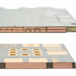
<img src="https://www.gopcba.com/wp-content/uploads/2021/04/ptt_contacts.jpg" alt="Impedance test coupon with labeled differential pairs” />
Designing the Test Coupon
A coupon is a structure on the panel that reproduces the impedance geometry of the product and can be measured without cutting the board. It should carry the same trace widths, the same layer spacing and the same reference planes as the design, and it should be placed where the process conditions match the product area.
Coupon design matters more than it is usually given credit for. A coupon with a wide ground plane and an isolated trace does not represent a dense routing area, and a coupon placed at the panel edge sits in a lamination environment that differs from the middle. The structure and its placement both belong in the fabrication notes, and the principles are described in our note on PCB test coupons.
Measurement by Time Domain Reflectometry
Time domain reflectometry sends a fast edge down the trace and records the reflection. The impedance is derived from the reflection coefficient along the length, so a single measurement shows the value and its variation along the trace. The technique is fast, and it is the one most suppliers use.
The measurement is sensitive to the launch. A connector or a probe that does not match the trace impedance creates a reflection at the start which can be mistaken for a trace defect, and a poorly calibrated reference plane shifts the whole result. Procedure and calibration matter more than the instrument.
Coupon Results and the Product
A coupon result describes the coupon. Whether it describes the product depends on how representative the coupon is and on whether the process is uniform across the panel. Where the coupon sits at a panel edge and the product sits in the middle, the two can differ by more than the tolerance.
That is why a supplier agreement should state the coupon design, its placement and the measurement method, and why a first article should include a measurement on the actual product geometry where possible. The board structure that supports those traces is described in our article on layer assignment.

Tolerance Stack Up and Yield
A tolerance of ten per cent does not mean that every board lands near the centre of the band. Width variation from etching is typically normally distributed, so a nominal design that sits exactly at the target will produce a distribution with half the boards above and half below, and a few outside the limits.
The practical response is to design the nominal value slightly off centre, so that the distribution sits inside the band rather than being centred on its edge. This is a deliberate choice and it has to be communicated to the fabricator, because the coupon will then also measure off centre.
Agreeing the Specification
A useful specification states the targets, the tolerance, the coupon design, the measurement method, the sample size and the action taken when a coupon fails. Without the last item, a failed coupon becomes a negotiation rather than a disposition.
It should also state which layers and which trace types are controlled. Applying a tolerance to every trace on a board is unnecessary and expensive, and applying it to none leaves the high speed signals to chance. The selection follows from the signal integrity analysis, which is a design task rather than a fabrication one.
Additional Considerations for This Build
Practical attention to impedance tolerance pays for itself here, because it decides whether the finished board behaves as the drawing intended. Where the requirement is not stated on the fabrication drawing or in the assembly notes, the shop has to assume a default, and that default is rarely the value the design was simulated with. Stating impedance tolerance explicitly, together with the tolerance that applies, removes the assumption and keeps the result predictable from batch to batch.
Process Control and Verification
On a design of this kind, test coupon is the item that decides how the rest of the board is arranged. Where a value sits close to a process limit, the drawing should say so, since the shop can then open the process window rather than working to a nominal figure that carries no tolerance. A stack-up that is drawn rather than described removes most of the ambiguity from a quotation, and it lets the fabricator price the board against the dielectric and copper weights that will actually be used.
Where the requirement is not written down, the shop supplies its own default, and the default is chosen for the process rather than for the design. The measurements that matter are the repeatable ones: conductor width and spacing, annular ring, finished hole size, plating thickness and surface finish are all verifiable on a coupon that travels with the panel.
Process Control and Verification
On a design of this kind, test coupon is the item that decides how the rest of the board is arranged. Where a value sits close to a process limit, the drawing should say so, since the shop can then open the process window rather than working to a nominal figure that carries no tolerance. A stack-up that is drawn rather than described removes most of the ambiguity from a quotation, and it lets the fabricator price the board against the dielectric and copper weights that will actually be used.
FAQ
Is ten per cent a reasonable tolerance? It is common for general high speed work and achievable in most shops. Tighter values are possible but reduce yield and increase cost.
Can impedance be measured on the finished board? It can be estimated from a coupon or measured with a probe, but a direct measurement of an assembled board is difficult because the launch changes. Coupon measurement remains the standard.
Does solder mask affect impedance? It does. A coating over a trace lowers the effective impedance slightly, which is why some specifications require the coupon to be measured with mask applied.