
Blind Via and Buried Via Fabrication Limits and Reliability
Blind and buried vias buy routing area on the layers below them, and they charge for it in fabrication stages, registration risk and inspection difficulty. The structures are buildable, but only inside aspect ratio limits that depend on the drilling method and on the dielectric being cut. This article covers those limits, the lamination sequence they impose, and the way the resulting joints are verified.
Definitions and What They Save
A blind via connects an outer layer to an inner layer without passing through the board, and a buried via connects two inner layers. Both free the surface for routing and allow a dense interconnect to be built without consuming a full layer for through holes.
The saving is routing area rather than size alone. Replacing a through via with a blind via frees every layer beneath it, and in a densely routed BGA escape pattern that difference often decides whether the design fits the layer count at all.
Aspect Ratio Limits by Drilling Method
Mechanical drilling produces blind vias at an aspect ratio of roughly one to one, while laser drilling handles much smaller diameters but is limited by the depth it can reach in a single step. Beyond those limits the hole is drilled in stages with an intermediate lamination.
The limit also depends on the dielectric. A resin coated copper or a thin prepreg stack accepts a deeper laser via than the same diameter in a glass reinforced core, because the glass and the resin do not vaporise at the same rate under the beam. The plating side of the same structure is covered in our hole copper notes.

The achievable aspect ratio is stated per material and per laser, so it belongs in the fabrication capability list rather than being treated as a constant of the process.
Lamination Sequence and Registration
A buried via has to be drilled and plated before the outer layers are laminated over it, so the board is built in stages. Each lamination adds a registration step, and registration error between stages is the dominant cause of a via landing off centre on its target pad.
Registration is measured with a coupon carrying targets on each layer, and the result is compared with the annular ring allowance. Where that allowance is tight, the drawing should state the layer to layer registration the process has to hold rather than relying on a default.
Via Fill and Planarisation
A blind via under a pad has to be filled and planarised, because an open hole beneath a BGA pad holds paste away from the joint. The fill is usually a conductive or non-conductive epoxy, cured and then ground back until the surface is coplanar with the copper.
The dimple limit after planarisation is commonly 25 micrometres, and the cap plating over the fill adds 5 to 8 micrometres of copper. Both numbers belong on the drawing, because the added copper changes the impedance of a via on a controlled net.
Reliability of Stacked Vias
Stacked vias, where one blind via sits directly on top of another, concentrate mechanical and thermal load in a column through the dielectric. Thermal cycling fatigues the copper at the junction between the vias, and the failure is a cracked barrel rather than a lifted pad.
Where stacking is used, qualification should include thermal cycling with resistance monitoring on a daisy chain routed through the stack. The number of cycles to a defined resistance rise is the figure that compares one construction with another, and the method is set out in our test design guide.
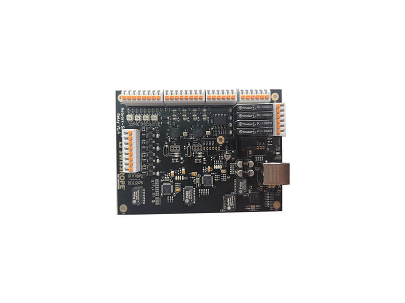
A daisy chain that passes through every stacked via in a coupon is worth more than a visual inspection, because the crack grows inside the dielectric where nothing can be seen.
Desmear and Plating in a Small Deep Hole
Before plating, the resin smear produced by drilling has to be removed, and the difficulty rises as the hole gets smaller. A permanganate desmear reaches a laser via readily but has to be controlled so that it does not attack the dielectric around the target pad.
Plating follows, and the throwing power of the chemistry decides how much copper reaches the floor of the via. A blind via with a thin floor is the defect to look for in a microsection, and it is invisible to any surface inspection.
Design Rules That Keep It Buildable
Design rules for blind and buried vias should state the drill diameter, the depth, the capture pad, the target pad, the registration allowance, the fill requirement and whether stacking is permitted. Each of those is a process limit rather than a preference.
The rules should also define the escape pattern. A fanout that puts a blind via in alternate pads is easier to build than one that puts a via in every pad, because the drill and the plating both have more room between holes.
Inspection and Verification
Blind and buried vias cannot be inspected from the surface, so verification is a microsection that includes the via floor, the plating thickness and the interface between fill and copper. The section is taken from a production panel rather than from a hand prepared sample. Radiographic methods are described in our X-ray and AOI guide.
X-ray confirms that the via is present and aligned, and shows voids in a filled via, but it does not measure plating thickness. The two methods together describe the construction, and neither is sufficient alone.
Cost and Documentation
Each additional lamination stage adds cost and lead time, so a stack-up with buried vias is priced against the layer count it saves rather than against a through via design. That comparison should include yield, because a complex build has more ways to fail.
The documentation that makes it workable is a stack-up drawing with the drill schedule per stage, a note on fill and planarisation, and the registration and impedance coupons that apply. Multi-stage builds of this kind are described in our multilayer processing notes.
The capture pad for a laser via is typically 0.15 to 0.2 mm larger than the via diameter, because the beam has to land inside the copper without breaking the dielectric around it.
Registration between a laser via and the target pad below is measured at four corners and the centre of the coupon, since the error is usually larger at the panel edges than in the middle.
A filled via under a pad is verified by section as well as by a surface measurement, because a plug that reaches only part of the barrel looks identical to a full one from above.
The number of lamination stages follows from the layer pairs that have to be connected, and each stage adds a cure cycle that the dielectric sees, so the total thermal exposure is reviewed with the stack-up.
Where the design permits a via to be stepped rather than stacked, the offset between the two spreads the strain and is a cheaper answer than changing the dielectric material.
FAQ
How deep can a laser drilled via go? It depends on the material and the laser, but the practical limit is around 0.8 to 1.0 of the via diameter, so a 0.1 mm via reaches roughly 0.1 mm of dielectric.
Are stacked vias reliable? They are used in volume production, but they concentrate thermal strain, so they should be qualified by cycling a daisy chain rather than by section alone.
Can a blind via be left unfilled? Only where it is not covered by a pad. Under a BGA pad the via has to be filled and planarised, or the paste is lost into the hole during printing.