Sizing Thermal Via Arrays Under High Power LED Pads
An LED converts only part of its input into light, and the rest becomes heat that has to leave through the board. Thermal vias are the standard way to move that heat from the pad under the die to a copper area on the other side, and their layout decides how much of the junction temperature is under control. This article explains how thermal via arrays work and how to size them against a real thermal requirement.
Why LEDs Need a Thermal Path Through the Board
The junction temperature of an LED sets both its light output and its life. A package that runs twenty degrees hotter than intended loses output and ages faster, and in a sealed enclosure the problem compounds because there is nowhere for the heat to go.
Heat leaves the die through the thermal pad on the package underside, so the board must present a low resistance path directly beneath that pad. The path is a chain of resistances, and the weakest link sets the die temperature. Copper provides heat spreading laterally, and vias carry it through the dielectric to a larger copper area that can dissipate it to the enclosure or to the air.
How a Thermal Via Array Works
Each via is a copper lined tube filled either with plating or with a filled and capped resin, and each provides a parallel path through a dielectric that is otherwise a good thermal insulator. Many small vias in parallel produce a much lower resistance than one large hole, because the copper volume scales with the wall area rather than with the hole area.
The array also spreads heat, so the temperature under the pad becomes more uniform. That matters for multi die packages, where a hot spot under one die shortens the life of the whole device. Uniform temperature across the pad keeps one die from driving the whole module.
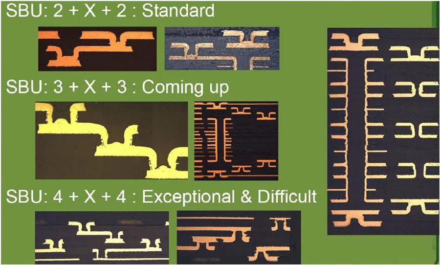
Vias must be placed inside the thermal pad area rather than around it, because heat travels through the shortest path and a ring of vias at the pad edge leaves the centre hot.
Via Size, Count and Pitch
Typical thermal vias range from 0.2 to 0.3 millimetres in finished diameter with a pitch of about one millimetre, though the right values depend on the dielectric thickness and the fabrication limit for the hole size you can plate reliably.
More vias lower the resistance but also consume pad area and complicate assembly, since solder can wick into open vias and starve the joint. Where vias are open, they are usually placed with a small offset from the pad edge or plugged and plated over to keep the mounting surface flat. A pitch that is too tight removes copper from the pad and weakens the solder joint.
Dielectric Thickness and Thermal Resistance
Thermal resistance through the board is proportional to dielectric thickness, so a thin dielectric helps as much as a dense via array. Standard FR-4 with a thin core performs better here than a thick stack, and laminates with higher thermal conductivity offer a further improvement.
Where the requirement is severe, the dielectric is often reduced to a thin layer under the LED area, using a separate thin core in the stackup. That keeps the rest of the board at normal thickness while giving the thermal path the shortest possible distance. Thinning the dielectric under the LED area is often the single most effective change available.
Copper Area on Both Sides
The vias move heat through the board, but they cannot dissipate it. The copper area on the far side performs that function, and its size, thickness and exposure to air determine how well the array works. A solid plane with good airflow is far more effective than a small isolated island.
Where the back side faces a metal enclosure, a thermal interface material can couple the board to the case, and the copper area then only has to be large enough to spread the heat evenly. In an enclosed plastic housing, the copper has to do the work through convection, which usually means more area and thicker copper.
Metal Core and Ceramic Alternatives
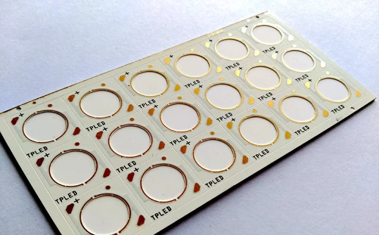
Metal core boards replace the dielectric with an aluminium or copper core separated from the circuit by a thin insulating layer. That layer is much thinner than standard laminate, so the thermal resistance drops substantially, and the core itself spreads heat across the whole board.
Ceramic substrates go further and remove the organic dielectric entirely, at higher cost and with a different set of mechanical constraints. The choice between them and a well designed thermal via array comes down to the junction temperature target, the power density and the acceptable cost per unit.
Manufacturing Limits for Filled Vias
Small vias in a thick board are difficult to plate evenly, and the aspect ratio sets the practical limit. A 0.2 millimetre hole in a 1.6 millimetre board has an aspect ratio of eight, which is manageable, but pushing beyond the shop’s capability produces voids in the wall that reduce thermal performance.
Filling and capping adds process steps and cost, but it gives a flat surface under the LED, which improves solder coverage. Where the thermal requirement allows, open vias with a careful stencil design are cheaper and work well enough. Where performance is critical, the extra process cost is usually justified by a lower junction temperature.
Measuring Junction Temperature
Junction temperature cannot be measured directly in a finished assembly, so it is inferred from a thermocouple on the board, from the case temperature, or from an optical measurement of the LED itself. Each method has its own offset, and the offset should be established once on a representative sample rather than assumed.
A practical approach is to build a thermal test board with the same copper area, via pattern and enclosure conditions as the product, then measure the board temperature at the LED pad under full load. That number, combined with the package thermal resistance, gives a usable estimate of the junction temperature.
Documenting the Thermal Design
The drawing should state the via diameter and pitch in the thermal pad area, whether the vias are filled and capped, the copper area on the far side and the dielectric thickness beneath the LED. Those values are part of the thermal design and cannot be changed by the shop without invalidating the calculation.
gopcb reviews thermal requirements with customers when the design calls for small vias, thin dielectric or filled and capped structures, because those features interact with plating capability and assembly, and a change in any of them is tracked in the thermal record. Settling them at the design stage keeps the thermal model valid and avoids a redesign after the first thermal measurement.
FAQ
How many thermal vias do I need under an LED? There is no universal count. Start from the junction temperature target, the dielectric thickness and the copper area available on the far side, then iterate until the calculated resistance meets the requirement.
Should thermal vias be filled and capped? Fill and cap gives a flat surface and better solder coverage, and it prevents solder from wicking away from the joint. Where the thermal requirement is modest, open vias with good stencil design can be sufficient.
Do open vias cause soldering problems? They can. Solder wicks into the barrel and may leave insufficient alloy under the pad, so open vias are usually placed with a small offset or plugged where the joint quality matters.