Voiding: Preparation, Placement and Process Control
Voids under a QFN thermal pad are the most common measured defect on modern assemblies, and they are also the one most often reported without context, because the number depends on how it was measured. The mechanism is straightforward and the corrections are known, but they have to be applied in the right order. This article covers the cause, the measurement and the four levers that change the result.
Why Voids Form Under a Thermal Pad
A QFN thermal pad is a large area of solder paste whose flux has to escape from the centre of it. As the alloy melts, the volatiles have a long path to the edge, and gas that does not escape remains as a void when the joint solidifies.
The void is not simply trapped air. Most of the volume comes from the flux vehicle, so the paste chemistry, the print pattern and the reflow profile change the result as much as the pad geometry does.
How Voiding Is Measured
Voiding is measured from an X-ray image by summing the void area inside the pad outline and dividing by the pad area. The number that results depends on the threshold used to define a void, so the threshold belongs in the specification. The method is described in our X-ray and AOI guide.
Typical limits are 25 percent total void area for general work, with some customers requiring 15 percent, plus a separate limit on the largest single void. Both numbers should be stated, because one large void disrupts the thermal path more than several small ones.

Void percentage is only comparable between images taken at the same threshold and the same magnification, so the settings belong in the inspection programme rather than in the operator’s judgement.
Stencil Aperture Pattern for a Large Pad
A single opening covering the whole thermal pad prints a solid block of paste with nowhere to vent. Dividing the aperture into a grid with 0.2 to 0.3 mm divisions reduces the volume and gives the flux a path to the edge.
The pattern also changes the printed volume, so the grid has to be designed against the target volume rather than applied as a fixed rule. A windowpane pattern with roughly 70 percent open area is a common starting point, adjusted after measurement. The aperture rules behind this are in our paste volume guide.
Paste Volume and Bond Line Thickness
The joint under a thermal pad is thin, and the paste volume is set so that the bond line finishes between about 0.05 and 0.1 mm. Adding paste does not improve the thermal path, because it is the bond line thickness that governs resistance, and the extra material only adds void potential.
On a large pad the stencil thickness and the aperture area together define the volume, and the print has to be verified on the product. Gasketing around a large aperture behaves differently from the fine pitch apertures elsewhere on the same stencil.
Reflow Profile and Flux Escape
A slow soak allows the flux to activate and the volatiles to leave before the alloy melts, which reduces voiding. A fast ramp reaches liquidus while the vehicle is still releasing gas, and the gas is then trapped by solidifying alloy. Zone settings that produce that shape are discussed in our zone settings guide.
Time above liquidus is the other factor, because a longer molten period lets voids coalesce and rise. The profile is therefore a balance between giving the flux time to escape and not keeping the joint molten longer than the paste allows.
Pad Geometry, Vias and Outgassing
A thermal pad containing vias gives trapped material a path downwards, but an unfilled via also absorbs paste during printing and releases volatile during reflow. Filling and capping the via removes both effects, as described in our via plugging guide.
Where via in pad is used, the dimple and cap figures matter for the same reason they do under a BGA. A void that forms above a plugged via is usually a sign of an incomplete cure rather than of a profile problem.
Component and Pad Surface Effects
Oxide on the board pad or on the package thermal pad changes the wetting, and poor wetting produces a joint that solidifies unevenly and traps flux in the areas that freeze last. Storage and handling of the components therefore affect voiding directly.
The package thermal pad itself is sometimes warped or has exposed copper, and both change the gap at the centre of the joint. A warped package gives a thicker gap on one side, which is typically where the void appears.
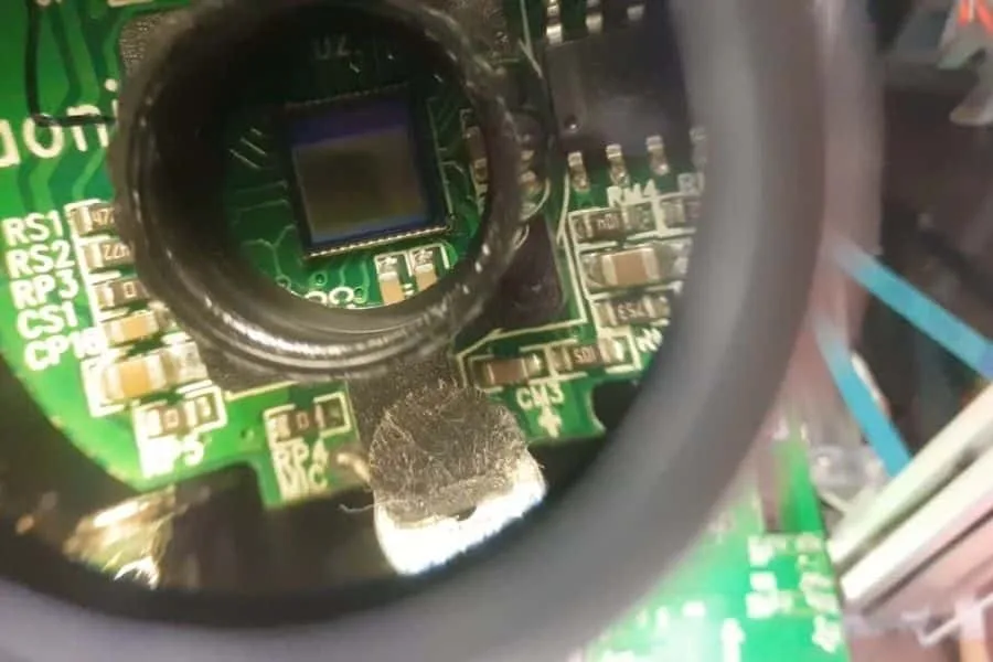
The component side of the joint is as variable as the board side, so a void that appears on one supplier’s parts and not another’s is a real finding rather than a measurement artefact.
Corrective Order
The first correction is the print: a divided aperture pattern with the correct volume fixes most voiding without any other change. The second is the profile, the third is the via structure, and only the last of these requires new boards.
Each change should be judged on a sample measured the same way, with the same X-ray threshold and the same pad outline. Comparing results taken with two different thresholds produces a change that does not exist.
Specifying Void Limits
The specification should state the total void area as a percentage of pad area, the maximum single void, the X-ray threshold used, and the sample size. Without the threshold and the sample size, two suppliers will report different numbers for the same joint.
Where voiding matters for thermal performance rather than appearance, the requirement can be written against a measured thermal resistance on a test vehicle. That links the number to the function, which is what the end customer is actually buying.
A windowpane aperture of nine or sixteen openings at about 0.25 mm division is a useful starting point, adjusted after the printed volume has been measured with an inspection system.
Where a no-clean paste is used, the flux that remains under the pad after reflow is part of the design, so the void limit is written against the residue the customer accepts rather than the paste supplier default.
Bond line thickness is confirmed by section on a sample after the first production run, because it is the thickness rather than the void area that decides the thermal resistance of the joint.
A board pad smaller than the package thermal pad concentrates paste at the centre, so the aperture pattern is designed against the smaller of the two dimensions.
Where the part is socketed rather than soldered, the void requirement does not apply, and the print is designed for contact rather than for a joint.
Cooling rate after liquidus changes the appearance of the fillet but not the void content measured by X-ray, so a change in cooling is not a change in voiding.
FAQ
What void percentage is acceptable? Twenty five percent of pad area is a common general limit and fifteen percent for thermally demanding parts, but the figure only means something when the X-ray threshold is stated with it.
Does more paste reduce voiding? No. Extra paste raises the bond line thickness and the volume of flux that has to escape, which usually increases voiding rather than reducing it.
Can voiding be fixed in reflow alone? Sometimes. A slower soak and a longer time above liquidus can remove much of it, but the aperture pattern is the cheaper and more repeatable correction.